

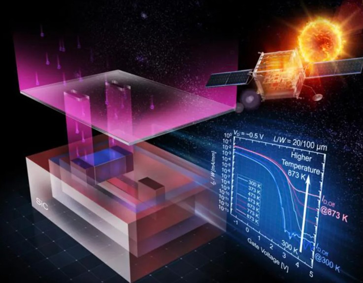
Researchers at Kyoto University in Japan have developed a silicon carbide transistor capable of operating normally at temperatures above 1,100°F, or 600°C. The advance could enable electronics to survive environments where conventional silicon components quickly fail, including the surface of Venus, where temperatures can reach about 860°F, tells Live Science.
The device is a silicon carbide junction field-effect transistor, or SiC-JFET. Silicon carbide has long been considered promising for high-temperature electronics, but existing JFETs suffer from poor controllability and excessive current leakage as temperatures rise. These problems have limited their practical use in spacecraft and other extreme environments.
The Kyoto team addressed both limitations by redesigning the transistor. Researchers placed the gate underneath the conducting channel in a bottom-gate configuration. This arrangement reduces changes in threshold voltage caused by dopant atoms penetrating farther into the silicon carbide than intended.
To control leakage, the researchers created two semiconductor wells around the transistor. The boundaries between these regions act as barriers that prevent unwanted current from bypassing the channel when the transistor is switched off, even as silicon carbide becomes more conductive at high temperatures.
Tests conducted from room temperature to 1,110°F showed stable transistor operation throughout the range. At about 750°F, the difference between the expected and measured threshold voltage remained below 0.1 volt.
The technology could have major implications for planetary exploration. Previous Venus landers survived only briefly, with the Soviet Venera 13 holding the record at 2 hours and 7 minutes. More heat-resistant electronics could help future probes operate longer without extensive cooling systems.
Applications extend beyond space. The transistors could work inside jet engines and other high-temperature industrial systems. Researchers must still integrate the devices into complex circuits, scale manufacturing to wafer level, and develop packaging capable of surviving extreme heat and pressure before practical deployment.
