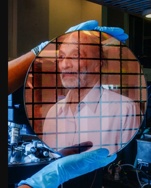
Artificial intelligence has shifted the semiconductor industry’s focus from simply making smaller transistors to finding better ways to combine multiple chips into powerful computing systems. At the center of this transition is advanced chip packaging, a technology that integrates processors, memory, and other components into a single high-performance module. Once considered a routine manufacturing step, packaging has become a strategic capability that now represents one of the biggest bottlenecks in AI chip production, tells The New York Times.
Electrical engineer Subramanian Iyer, a longtime pioneer in advanced packaging, warns that the United States has become heavily dependent on Taiwan Semiconductor Manufacturing Company (TSMC), which controls an estimated 95% of advanced packaging capacity. TSMC’s CoWoS technology allows companies such as Nvidia to combine multiple AI processors with stacks of high-speed memory into a single package containing hundreds of billions of transistors. However, demand for CoWoS already exceeds production capacity by about 30%, creating supply constraints that threaten the expansion of AI infrastructure.
The challenge extends beyond manufacturing capacity. Although TSMC is building advanced fabrication plants in Arizona, chips produced there must still be shipped to Taiwan for packaging until CoWoS capabilities are introduced later this decade. This leaves the United States vulnerable despite billions of dollars invested through the CHIPS and Science Act to strengthen domestic semiconductor production.
Recognizing the growing importance of packaging, several U.S. companies are expanding their investments. Intel is strengthening its advanced packaging business, Applied Materials is building a $5 billion research facility that includes packaging technologies, and Amkor Technology is constructing its first U.S. packaging plant in Arizona with support from Nvidia and Apple. At the same time, startups are pursuing alternative packaging approaches that reduce reliance on complex silicon interposers and expensive manufacturing processes.
Government policy remains uncertain. A proposed $1.1 billion packaging research center in Arizona, championed by Iyer under the CHIPS Act, was abandoned after changes in federal priorities. While industry leaders disagree on where such research should be conducted, most agree that sustained investment is essential.
The article argues that advanced packaging has become just as important as chip fabrication itself. As AI processors continue to grow in complexity, leadership in packaging technology may prove decisive in determining the future balance of global semiconductor innovation and supply chain resilience.