
AI agents are beginning to reshape semiconductor engineering, but capable language models alone cannot deliver autonomous chip design. Based on Nvidia’s Karthik Chandrasekaran’s presentation at DAC 2026, ChipAgents describes three technologies needed to create AI-native workflows: accelerated computing, AI physics, and AI agents.
The first requirement is faster engineering computation. Semiconductor simulations for circuit behavior, power, thermal effects, electromigration, and other physical phenomena can take hours or days. Such delays limit agents that need rapid feedback to evaluate design changes. GPU acceleration using CUDA, CUDA-X libraries, and multi-GPU systems can shorten these workloads, allowing engineers and agents to test more alternatives.
AI physics offers another route. High-fidelity simulations can generate training data for surrogate models that learn to approximate physical behavior. Once trained, these models could predict temperature, stress, electromagnetic fields, IR drop, and reliability metrics in seconds rather than repeatedly running expensive simulations. Applications extend from chip design and manufacturing to advanced packaging and system-level engineering.
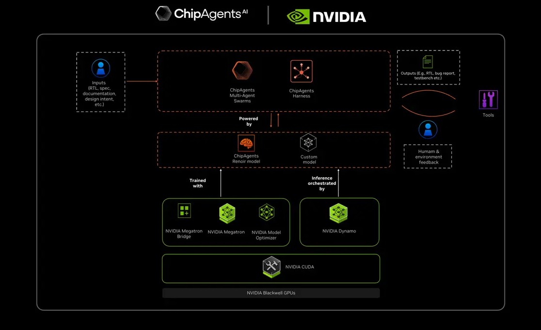
The third component is agentic AI. Rather than simply generating RTL or answering engineering questions, agents can access specifications, constraints, previous runs, reports, layouts, and other design information. They can then interact with simulation, verification, synthesis, place-and-route, and signoff tools to gather evidence and determine their next action.
This closed-loop process is particularly important because semiconductor development requires repeated iteration. An agent might generate RTL, run simulations, identify failures, investigate causes, modify the design, and test again while preserving results from previous attempts.
ChipAgents envisions multi-agent systems operating within this framework, connecting design intent and engineering knowledge with EDA tools, physics models, and human feedback. The goal is an environment where AI continuously works toward measurable engineering objectives rather than performing isolated tasks.
Together, faster computation, physics-aware AI, and long-running agents could shift semiconductor development from AI-assisted automation toward AI-native engineering spanning the complete journey from physics to silicon.
