

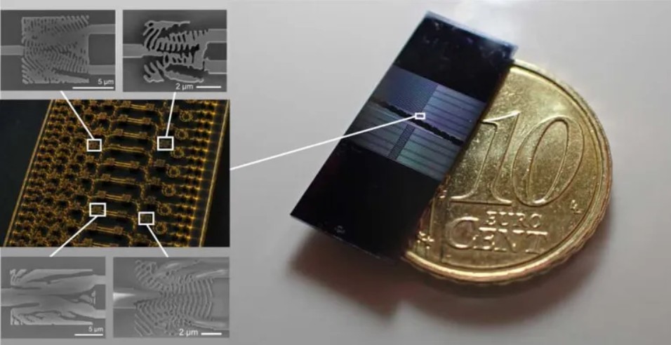
Researchers have used artificial intelligence to design three photonic chip components up to 500 times smaller than conventional versions. The devices measure only a few micrometers and demonstrate how AI-driven design could increase the number of functions engineers can integrate into photonic circuits, tells Live Science.
Unlike conventional microchips, which process information using electrons, photonic chips use photons. Light can transmit information rapidly, support multiple data streams through different wavelengths, and produce less waste heat. These characteristics make photonic chips useful for fiber-optic communications, data centers, artificial intelligence, lidar, and quantum computing.
Photonic circuits use waveguides to direct light and require components such as wavelength splitters, spatial mode sorters, and mirrors. Researchers applied an AI-based inverse-design method to shrink all three. Instead of manually developing a structure, engineers specified the optical performance they wanted and added manufacturing constraints. The algorithm then worked backward, repeatedly testing geometries until it identified structures capable of producing the required behavior.
The researchers fabricated the components from silicon nitride roughly 400–800 nanometers thick. The resulting mirrors measure about 11 micrometers long and reflect up to 98.5% of incoming light while suppressing unwanted light patterns. The wavelength splitter measures about 5 micrometers across, approximately the size of a bacterium, while the spatial mode sorter is slightly larger.
Beyond miniaturization, the research shows that AI can explore geometries that engineers might not consider using conventional design methods. The additional chip space could allow designers to integrate more components and introduce new capabilities without increasing overall chip size.
The researchers have demonstrated the three devices individually but have not yet integrated them into a complete optical circuit. That is the next challenge. If successful, the approach could support denser, scalable photonic systems while showing that AI-generated designs can remain practical to manufacture.
