

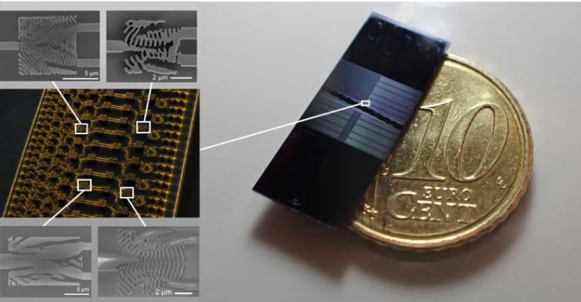
Researchers have used artificial intelligence to design three photonic chip components that are up to 500 times smaller than conventional versions. The resulting nanostructures go beyond geometries typically conceived by engineers while remaining practical to manufacture, tells Live Science.
Unlike conventional microchips, which process information using electrons, photonic chips use photons. Light-based processing can provide faster data transmission, greater bandwidth, and lower heat losses. These advantages make photonic chips useful for fiber-optic communications, data centers, artificial intelligence, lidar, and quantum computing.
The researchers focused on wavelength splitters, spatial mode sorters, and mirrors, components responsible for directing and manipulating light inside photonic circuits. Instead of manually refining established designs, the team used an inverse-design algorithm. Researchers specified what each component should accomplish and supplied manufacturing constraints. The AI then worked backward, repeatedly testing and optimizing possible nanostructures until it identified geometries capable of delivering the required optical performance.
The team also fabricated the components from relatively thick silicon nitride, between roughly 400 and 800 nanometers thick. This material configuration reduces light loss and improves wavelength confinement. The resulting mirrors measure about 11 micrometers long yet reflect as much as 98.5% of incoming light while rejecting unwanted light patterns. Paired mirrors allowed light to bounce more than 100 times before escaping. The wavelength splitter is only about 5 micrometers across, roughly the size of a bacterium.
Smaller components could allow engineers to fit significantly more functionality onto individual photonic chips. However, the researchers have demonstrated the devices individually and have not yet integrated them into a complete optical circuit.
The next challenge is combining these AI-designed components into functional photonic systems. If successful, the approach could support denser, higher-performance chips while reducing the time required to explore unconventional designs, opening possibilities for communications, AI computing, autonomous vehicles, and quantum technologies.
