

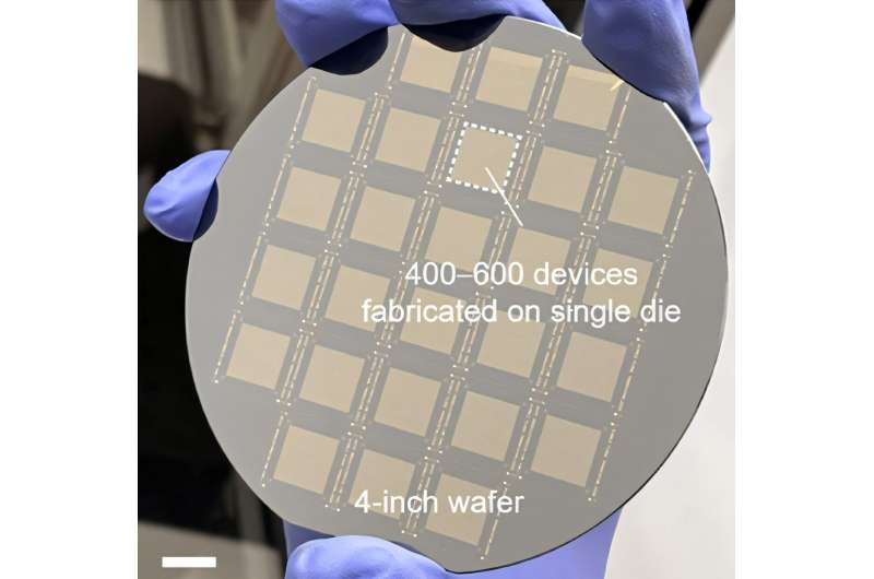
Researchers at the Korea Advanced Institute of Science and Technology (KAIST) have developed an automated platform that could dramatically accelerate the discovery and evaluation of two-dimensional (2D) semiconductors for future low-power AI chips. The system replaces the slow, manual process of locating microscopic semiconductor flakes and fabricating test devices with an automated workflow that identifies promising materials, designs transistor layouts, and analyzes device performance at scale. The advance is expected to shift semiconductor research from trial and error toward a faster, data-driven approach, tells Tech Xplore.
Two-dimensional semiconductors, such as molybdenum disulfide (MoS₂), are only a few atomic layers thick and are widely regarded as potential successors to silicon in advanced electronics. Their ultrathin structure could enable smaller, faster, and more energy-efficient chips for applications including artificial intelligence, smartphones, wearable electronics, data centers, and medical sensors. However, because each semiconductor flake varies in size, location, and thickness, researchers have traditionally spent considerable time identifying suitable samples and manually designing test devices.
The KAIST team automated this process by using optical microscope images to detect semiconductor flakes based on subtle variations in their red, green, and blue color values, which change with material thickness. The system then automatically generated electrode designs and fabricated transistors for testing. Verification with atomic force microscopy confirmed that the platform could accurately distinguish flakes with thicknesses ranging from three to eight atomic layers. Using this workflow, the researchers screened more than 120,000 semiconductor flakes and fabricated and analyzed 1,615 transistors.
The large dataset also revealed a previously difficult-to-verify relationship between thickness and electrical performance. As the semiconductor layers became thicker, electrical current flowed more easily, but the devices became less effective at switching current on and off. Such statistically significant findings would have been difficult to obtain through conventional small-scale experiments.
Beyond automating fabrication, the platform establishes a foundation for AI-assisted materials discovery. By rapidly generating large volumes of experimental data, researchers can more efficiently identify promising semiconductor materials and eventually train AI systems to design new ones. The technology could shorten the path from laboratory research to commercial low-power electronics while supporting the continued development of next-generation AI semiconductors.
