

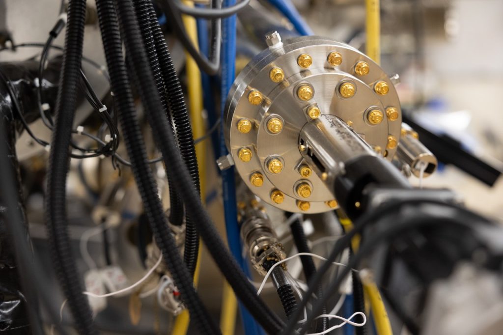
As semiconductor devices continue to shrink, silicon is nearing the physical limits of its performance. Researchers at Virginia Tech are exploring alternative semiconductor materials that can overcome these limitations and support the next generation of electronic and photonic technologies. Ph.D. student Sengunthar Karthikeyan, a member of the Advanced Devices and Sustainable Energy Laboratory (ADSEL), is at the forefront of this effort, investigating new material systems that could transform the design of transistors, lasers, and photodetectors.
Semiconductors serve as the foundation of modern computing by controlling the flow of electricity through billions of microscopic switches. However, continued miniaturization has introduced challenges such as electron tunneling, excessive heat generation, and silicon’s inability to efficiently emit light. These limitations make it increasingly difficult to improve the performance of conventional silicon-based devices.
Working with Professor Mantu Hudait and fellow researchers, Karthikeyan is developing semiconductor materials using combinations of indium, gallium, aluminum, arsenic, germanium, and tin. These engineered materials, including indium-gallium-aluminum-arsenic with germanium-tin and mechanically strained germanium, offer the potential for higher operating frequencies, faster switching speeds, and improved support for quantum-scale applications. They also make it possible to integrate electronic and photonic components on a single platform.
The research demands precision and persistence. In one project, Karthikeyan spent nearly 14 hours carefully etching through semiconductor layers to reach an interface only a few nanometers thick. Although his first attempt missed the target, he repeated the experiment and successfully collected data that contributed to his first published paper on lattice-matched germanium-tin materials with enhanced carrier confinement for future laser and photodetector applications.
Following an internship at Intel, Karthikeyan plans to enter the semiconductor industry, where he hopes to translate advanced materials research into manufacturable technologies. His long-term vision is to enable transistors, lasers, and photodetectors to be fabricated together on a single semiconductor wafer, paving the way for faster, more efficient, and highly integrated computing systems.
