

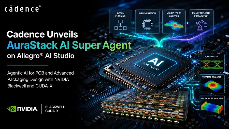
SAN JOSE, CA, July 16, 2026 – Cadence has added the AuraStack AI Super Agent to Allegro AI Studio, bringing agentic AI workflows to PCB and advanced packaging design. The system uses NVIDIA Blackwell and CUDA-X to coordinate AI agents across planning, implementation, multiphysics analysis and manufacturing preparation.
AuraStack builds on the architecture behind Cadence’s ChipStack AI Super Agent. It combines agentic AI with simulation and optimization tools for design exploration, implementation and signoff. The product extends Cadence’s AI agent portfolio across digital and analog silicon design, packaging and PCB design, alongside ChipStack, InnoStack and ViraStack AI Super Agents.
The system covers planning, constraints management, physical structure definition, IP creation and reuse, place and route, design for manufacturability and multiphysics analysis. AuraStack models electrical, thermal and mechanical behavior, including SI/PI, thermal performance, mechanical stress, drop, vibration and fatigue analysis, within a closed-loop environment.
“The next era of AI infrastructure – spanning data centers, automotive, aerospace and physical AI – will be defined not only by silicon, but by the systems that connect, power and cool it,” said Michael Jackson, corporate vice president of R&D for system design and analysis at Cadence. “As hyperscale data centers deploy massive AI clusters and other industries advance increasingly intelligent, high-performance systems, engineering teams face growing complexity in PCB and advanced package design. Agentic AI orchestration, combined with trusted EDA and SDA tools, enables customers to move from manual iteration to intelligent, automated design realization.”
Cadence said the continuous multiphysics feedback loop lets engineering teams evaluate trade-offs earlier in the design process and reduce late-stage rework.
The AuraStack AI Super Agent’s benefits include:
- Shortening time to market by 2X, with 15X productivity and multiphysics-driven quality through automated design tasks and design exploration.
- Giving engineering teams a shared, multiphysics-aware design environment across domains.
- Supporting early and continuous multiphysics co-optimization to reduce late-stage rework and design iterations.
- Unifying Cadence multiphysics signoff tools, including Celsius Thermal Solver, Clarity 3D Solver for 3D-EM, MSC Nastran and Marc Linear and Non-Linear Finite Element Analysis Solvers for mechanical analysis, and Sigrity X Platform for signal and power integrity.
- Identifying system issues earlier in development to limit respins.
- Supporting product-level optimization, including co-optimization with advanced packaging approaches
Cadence is working with NVIDIA, TSMC, Socionext, FORVIA HELLA and Schneider Electric on AuraStack-related workflows for IC packaging and PCB design.
NVIDIA is using Cadence tools to automate system design workflows.
“The scale and complexity of modern AI infrastructure demands a new design approach,” said Tim Costa, vice president and general manager of computational engineering at NVIDIA. “NVIDIA’s collaboration with Cadence is advancing AI-powered engineering workflows that accelerate design convergence and innovation across the industry. The Cadence AuraStack AI Super Agent and the Millennium M2000 Supercomputer deliver up to 20X faster multiphysics performance, giving our engineers the capability to tackle the most demanding design challenges and bring the next generation of AI infrastructure to life.”
Cadence is partnering with TSMC on AI-driven automation for package implementation in multi-die systems.
“As advanced packaging complexity grows, customers need new levels of automation to achieve timely design convergence,” said Aveek Sarkar, director of the ecosystem and alliance management division at TSMC. “Our long-standing partnership with Open Innovation Platform® (OIP) ecosystem partners like Cadence to deliver advanced package design and verification solutions for TSMC 3DFabric® technologies helps customers accelerate the realization of next-generation multi-die systems for AI and high-performance computing applications. Through our multi-year collaboration on substrate auto routing, we are already enabling customers to boost productivity by 100X while delivering quality of results similar to manual routing.”
Socionext is using Cadence tools to automate and optimize semiconductor package and PCB design workflows.
“AI-driven agents are set to transform IC package and PCB design by automating SI, PI and thermal workflows and enabling generative design,” said Iwasaki Toshifumi, lead design execution leading unit, global leading group at Socionext Inc. “This acceleration allows our engineers to focus on higher-value work like architecture exploration, margin optimization, and multiphysics tradeoffs, while capabilities such as automated routing and chip-package-board co-design accelerate convergence and reduce manual effort.”
FORVIA HELLA is using Cadence AI-assisted placement technology in automotive electronics development.
“Working closely with Cadence has fundamentally changed the way FORVIA HELLA develops advanced automotive electronics. Using AI-assisted placement technology, a task involving the placement of 300 components that previously took up to four days can now be completed in just four minutes,” said Sven Hoenecke, president & CEO, electronics NSA at FORVIA HELLA. “This step change in productivity allows our engineers to evaluate more design alternatives, optimize layouts earlier in the development process, and accelerate the development of innovative products without compromising quality. By automating repetitive work, our teams can focus more time on solving complex engineering challenges and bringing new technologies to market faster.”
Schneider Electric is working with Cadence on AI-driven design automation and engineering knowledge capture for electronic design workflows.
“At Schneider Electric, we see AI as much more than a productivity tool. Our collaboration with Cadence has demonstrated the potential of AI to accelerate design activities and improve engineer efficiency,” said Daniel Gheno, senior vice president, innovation and technology EM at Schneider Electric. “The next frontier is to combine design automation with engineering expertise, enabling companies to capture decades of know-how and make robust design decisions available to every engineer. We believe this is where AI can truly transform electronic design.”
Source: Cadence
About Cadence

Cadence Design Systems is a U.S.-based technology firm that develops electronic design automation (EDA) tools, hardware, and IP for designing integrated circuits and electronic systems. Formed in 1988 through the merger of SDA Systems and ECAD, the company is headquartered in San Jose, CA. Cadence provides software and solutions for designing SoCs, PCBs, and complete electronic systems used in the semiconductor, automotive, aerospace and defense, telecommunications, and consumer electronics industries. Its tools support both digital and analog design workflows. Cadence employs about 12,000 people globally.
