

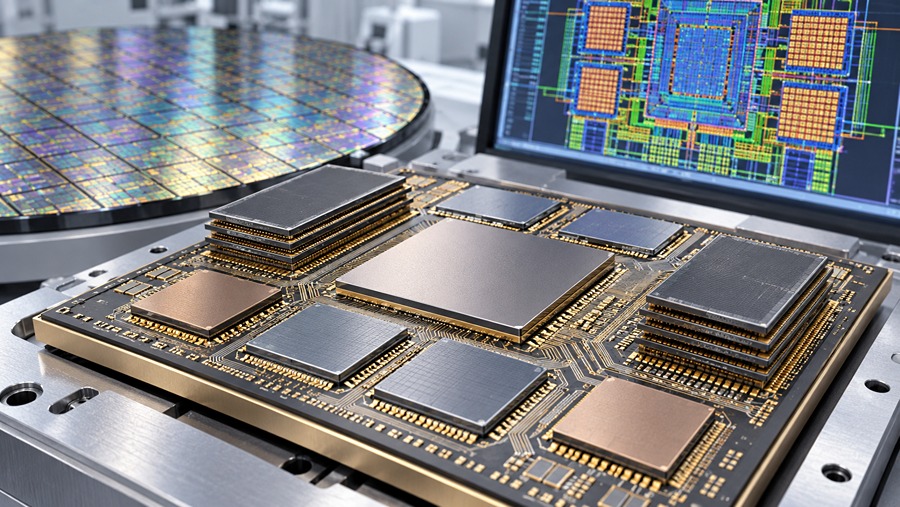
SAN JOSE, CA, Sep 25, 2026 – Cadence has secured design tool certifications for TSMC’s A14, A16 and N2P processes through an expanded partnership. The collaboration also covers silicon-proven IP and 3DFabric support for wafer-scale systems containing chiplets.
The companies are supporting agentic AI chip and 3D-IC design flows across TSMC’s N3, N2, A16 and A14 technologies. Cadence also demonstrated a UALink implementation on N3P and introduced silicon-proven IP for N3P and N2P. The work supports AI and high-performance computing designs.
“Cadence’s partnership with TSMC continues to deliver breakthrough innovations that enable leading‑edge customers to accelerate their most advanced semiconductor designs,” said Chin‑Chi Teng, senior vice president and general manager of the digital and signoff group at Cadence. “With AI‑driven design flows, silicon‑proven IP and 3D-IC solutions, we’re helping customers achieve faster time to market and improved PPA on TSMC’s leading‑edge process technologies.”
“TSMC, together with our Open Innovation Platform (OIP) partners like Cadence, is addressing the key demands of semiconductor development to achieve higher performance and energy efficiency in AI systems,” said Aveek Sarkar, director of the ecosystem and alliance management division at TSMC. “With broad collaboration on AI-based solutions, our longstanding partnership is further accelerating our mutual customers’ journey of expanding AI with leadership silicon.”
A14 and A16 Design Tool Certification
The A14 and A16 certifications cover Cadence’s digital, signoff and custom/analog design flows. The digital flow includes Innovus Implementation System and Cadence Cerebrus Intelligent Chip Explorer for design-technology co-optimization. The tool set also includes Genus Synthesis Solution, Tempus Timing and ECO Solution, and EMX Planar 3D Solver. Other tools include Voltus IC Power Integrity Solution, Quantus Extraction Solution, Pegasus Verification System and Liberate Characterization Portfolio.
For custom and analog designs, Virtuoso Studio supports layout generation that follows design rules and automated migration to A16 and A14. Applications include AI, HPC and mobile systems-on-chip (SoC).
Cadence has taped out UCIe-64G IP on A14 and is developing LPDDR6 IP. The company has also prioritized development of HPC and AI memory IP and other protocols for compute chiplets.
Artisan Foundation IP and mixed-signal IP for A14 remain in development, with availability expected in Q4, 2026. These include standard cells, GPIO and memory compilers for HPC, AI and networking applications.
N2P Design Flows and IP
Cadence’s N2P certification covers analog, digital and signoff flows for infrastructure and physical AI applications. Virtuoso Layout Suite includes connectivity models for custom design.
N2P IP tape-outs include DDR5, LPDDR5 and PCIe 6.0. Cadence expects PCIe 3.0 IP to tape out in Q4, 2026. UCIe-64G IP on N2P silicon is undergoing laboratory testing, while Cadence has characterized the IP on N3P.
3DFabric and COUPE Integration
Cadence supports the TSMC SoW-X design flow for wafer-scale systems. Its tools also support CoWoS-L-style packages measuring five times the reticle size.
Integrity 3D-IC platform handles system planning and assembly. It supports integration of SoIC, eDTC, MIMCap, integrated voltage regulators, HBM logic base dies and substrates.
An automatic routing flow driven by pre-simulation is now certified using Allegro Substrate Router and OmniRoute Interconnect Router. The flow derives routing strategies for signal integrity across CoWoS architectures to address UCIe requirements.
TSMC-COUPE (Compact Universal Photonic Engine) supports integration with Cadence’s 224G SerDes IP for photonic-to-silicon connectivity. The SerDes IP aligns with UALink, ESUN, UltraEthernet and optics technologies.
Cadence’s HPC and AI IP portfolio includes HBM4/4E, LPDDR6/5X, DDR5-MRDIMM, PCIe 7.0 and UCIe 64G.
Global Unichip Design Work
Global Unichip Corp. uses Cadence tools to develop silicon for AI accelerators and hyperscale systems on TSMC processes. Cadence says its automation helps GUC manage scheduling risks when adopting new process technologies.
“As designs scale to leading‑edge TSMC process technologies such as N3P and N2P, success depends on tightly optimized execution across increasingly complex system requirements – especially when working with the early‑adopters where schedule risk is highest,” said Louis Lin, senior vice president at Global Unichip Corp. “Cadence’s solutions provide the predictability, performance and silicon correlation we need to successfully deliver and tape out complex designs on TSMC’s most advanced nodes.”
Source: Cadence
About Cadence

Cadence Design Systems is a U.S.-based technology firm that develops electronic design automation (EDA) tools, hardware, and IP for designing integrated circuits and electronic systems. Formed in 1988 through the merger of SDA Systems and ECAD, the company is headquartered in San Jose, CA. Cadence provides software and solutions for designing SoCs, PCBs, and complete electronic systems used in the semiconductor, automotive, aerospace and defense, telecommunications, and consumer electronics industries. Its tools support both digital and analog design workflows. Cadence employs about 12,000 people globally.
