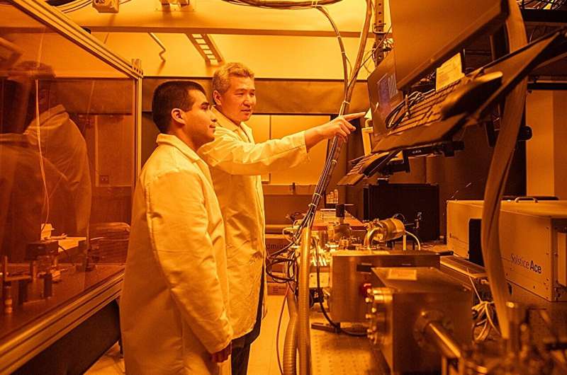
Researchers have demonstrated a low-cost technique that could make semiconductor fabrication more accessible by transforming a desktop 3D printer into a tool capable of producing microscale patterns, tells Tech Xplore. The work addresses one of the biggest barriers in electronics research: the high cost and complexity of equipment required for semiconductor manufacturing.
Traditional semiconductor fabrication relies on photolithography systems that can cost hundreds of thousands or even millions of dollars. These tools are essential for creating the intricate patterns used in integrated circuits, sensors, and microelectronic devices. As a result, access to chip fabrication technologies is often limited to well-funded laboratories and industrial facilities.
The new approach repurposes a commercially available resin-based 3D printer and modifies it to perform precision patterning at much smaller scales than those typically associated with additive manufacturing. By carefully controlling light exposure and optimizing printing parameters, the research team was able to create fine features suitable for semiconductor and microelectronics applications.
According to the researchers, the technique enables rapid prototyping of microscale structures without requiring expensive clean-room infrastructure. The system can produce detailed patterns that may be used in the development of electronic components, microfluidic devices, sensors, and other research applications. Because the equipment is relatively inexpensive and widely available, the method could broaden access to advanced fabrication capabilities for universities, startups, and smaller laboratories.
The project reflects a broader trend toward democratizing semiconductor research through lower-cost manufacturing tools. While the modified printer cannot match the precision required for leading-edge commercial chips, it offers sufficient resolution for many experimental and educational applications. Researchers can test concepts, iterate designs quickly, and conduct fabrication-related research without relying on specialized facilities.
The team believes the technique could accelerate innovation by reducing both cost and development time. It may also serve as a training platform for students learning semiconductor manufacturing principles. As demand for electronics and chip-related expertise continues to grow, accessible fabrication tools could help expand participation in the field.
The work demonstrates that advances in consumer hardware can sometimes be adapted for sophisticated scientific purposes, opening new possibilities for semiconductor research outside traditional manufacturing environments.