Researchers at the University of Illinois Urbana-Champaign have developed a new manufacturing approach that could accelerate the development of monolithic three-dimensional integrated circuits, a long-sought technology capable of dramatically increasing chip density while reducing energy consumption, tells Tech Xplore. Published in Nature, the work addresses one of the biggest obstacles to stacking transistors vertically on a single chip: heat.
Conventional computer chips arrange transistors side by side on a flat silicon wafer. By stacking multiple layers of transistors on top of one another, engineers could significantly increase computing power without increasing a chip’s footprint. However, fabricating additional transistor layers typically requires high-temperature processing that can damage or destroy circuitry already built beneath them.
Previous attempts to overcome this challenge often relied on replacing silicon with alternative semiconductor materials that could be processed at lower temperatures. While these approaches reduced thermal stress, they generally delivered lower performance than traditional silicon devices, limiting their practical value.
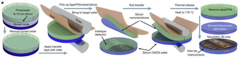
The Illinois research team, led by Qing Cao, took a different approach. Rather than abandoning silicon, they developed a method for transferring ultrathin silicon sheets only 10 nanometers thick onto existing chip layers. These flexible sheets are peeled from a specialized silicon substrate using adhesive tape and then rolled onto the chip surface at temperatures below 200°C, a threshold safe for previously fabricated circuitry.
Because the silicon layers are extremely thin and flexible, they can conform to uneven surfaces while maintaining a uniform bond. The researchers also designed transistor structures that avoid the high-temperature processing steps typically required in conventional transistor fabrication.
The resulting devices achieved electrical performance comparable to standard silicon transistors while allowing successive layers to be aligned with precision better than 10 nanometers. Using the technique, the team successfully fabricated three-layer memory cells that reduced circuit area by as much as three times compared with equivalent planar designs.
Although scaling the process to industrial wafer sizes remains a significant challenge, the study demonstrates that high-performance silicon can remain central to future 3D chip architectures. The advance represents an important step toward denser, more energy-efficient integrated circuits built using materials and technologies already familiar to the semiconductor industry.