
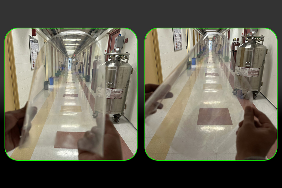
MIT researchers have developed a scalable fabrication process for silicon-photonics chips that are both flexible and transparent. The advance could extend photonic technology into applications such as body-conforming health monitors and curved augmented reality displays while retaining compatibility with established semiconductor manufacturing, tells MIT News.
Silicon photonics uses light rather than electricity to transmit and process information on chips. Existing manufacturing techniques can produce 300-millimeter wafers containing billions of nanoscale optical devices, but the resulting chips are typically rigid and opaque. Previous demonstrations of flexible or transparent photonic chips were also difficult to manufacture at scale.
Working with engineers at NY Creates’ Albany NanoTech Complex, the MIT team addressed this limitation using standard foundry tools. Researchers first pattern optical waveguides on a conventional silicon substrate. They temporarily bond another silicon wafer to the structure, flip it, and remove the original substrate until only ultrathin oxide and waveguiding layers remain.
A transparent polyester film is then attached before the temporary support is removed. The result is a flexible, transparent wafer only a few microns thick.
Manufacturing such thin structures required careful control of mechanical stress. Warping could create ripples or even shatter a wafer during processing. The team therefore limited processing temperatures to 500°C or below and combined industrial silicon-thinning techniques with precise chemical etching.
Tests demonstrated the platform’s durability and optical performance. A chip was bent thousands of times around cylinders, including one about the width of a small screw, without performance degradation. Transparency tests using a bionic-eye setup found minimal haze and little noticeable image distortion.
Potential applications include transparent displays integrated into windshields or pilots’ visors and discreet wearable devices. The researchers now plan to incorporate more complex components while improving waveguide efficiency and transparency, bringing flexible photonic systems closer to practical use.
