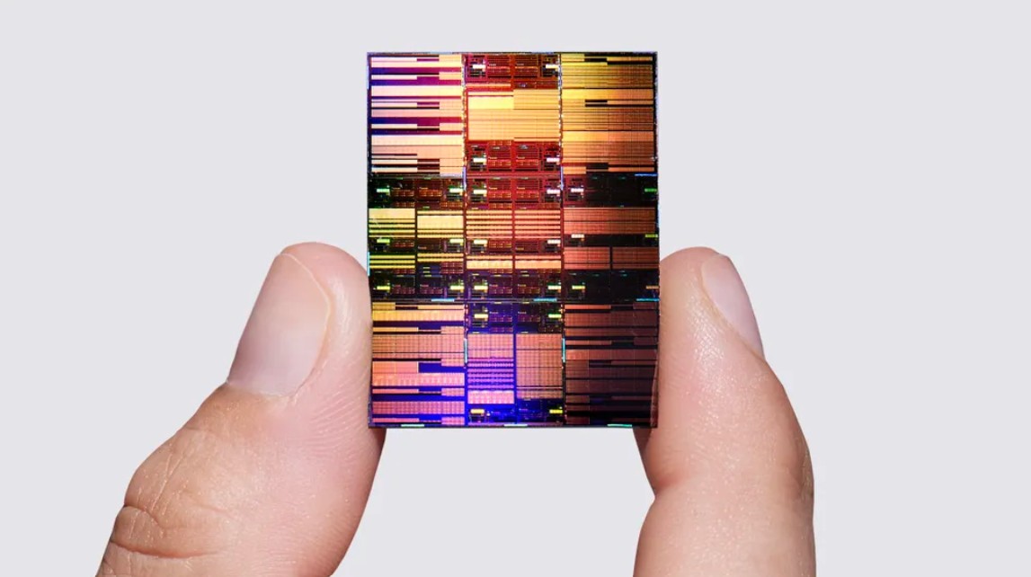
IBM has unveiled what it describes as the world’s first sub-1 nanometer semiconductor technology, introducing a 0.7 nanometer transistor architecture that could extend the life of silicon chips well beyond current manufacturing limits. The breakthrough centers on a new design called NanoStack, which replaces conventional nanosheet transistors with vertically stacked structures, allowing engineers to pack significantly more transistors into the same chip area, tells Live Science.
The prototype demonstrates that nearly 100 billion transistors can fit into a chip roughly the size of a human fingernail, almost double the density of today’s leading 2 nanometer designs. According to IBM, this architecture could deliver up to 50% higher performance while reducing energy consumption by as much as 70% compared with current semiconductor technology. Those gains could benefit AI accelerators, supercomputers, cloud infrastructure, and graphics processors that demand ever greater computing power without proportionally increasing power consumption.
One of the most striking aspects of the announcement is IBM’s long-term roadmap. Researchers believe NanoStack could eventually enable transistors measuring just 0.1 nanometers, approaching atomic dimensions. At these scales, engineers measure device features in angstroms rather than nanometers, highlighting how close semiconductor manufacturing is moving toward the physical limits of matter. Achieving commercial production at that scale will require overcoming significant manufacturing and economic challenges, and IBM acknowledges that the technology remains in the research stage.
IBM no longer manufactures chips itself, but it has a history of licensing its semiconductor innovations to commercial foundries. The company expects NanoStack to follow a similar path once the technology becomes practical for large-scale production. By continuing to advance classical semiconductor research alongside its investments in quantum computing, IBM aims to shape the next generation of computing hardware. The development also suggests that Moore’s Law, long considered to be nearing its end, may still have room to evolve through new transistor architectures rather than simple dimensional scaling.