

As computer chips become smaller and more powerful, managing the heat generated by densely packed transistors is becoming a major engineering challenge. MIT researchers have developed a new technique that can precisely track heat movement through individual layers of electronic materials, potentially helping engineers design more powerful and energy-efficient devices.
Existing thermal measurement techniques have important limitations. Optical methods such as time-domain thermal reflectance cannot easily examine buried layers in devices containing multiple materials. Infrared cameras also lack the spatial resolution and speed required to capture tiny, rapid thermal changes.
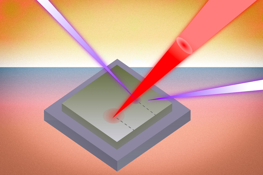
The MIT team addressed these limitations by combining laser pulses with ultrafast X-rays. A laser heats the sample, while a tightly focused X-ray beam penetrates multiple layers and tracks changes as the heat dissipates. The approach allows researchers to observe thermal transport at extremely small scales and distinguish what happens within individual layers and across their interfaces.
Researchers tested the method on a device consisting of gallium nitride layered on silicon. Gallium nitride is considered promising for electronics because of its thermal properties, but microscopic defects introduced during manufacturing can reduce its ability to transfer heat.
Measurements revealed that a micron-scale wrinkle defect caused a fourfold reduction in heat dissipation. Heat movement across the materials also dropped by 25%. The defect caused heat to travel unevenly, demonstrating that imperfections can influence thermal behavior more dramatically than conventional models of ideal crystals suggest.
The technique could give engineers experimental data for designing electronics that handle heat more effectively. Researchers could examine the influence of material choices, interfaces, geometry, and manufacturing defects instead of relying primarily on averaged measurements or idealized simulations.
The team expects the method to apply to many materials and devices. A semiconductor industry consortium has already expressed interest in using the technique to study chips, pointing to potential applications in AI hardware, wearables, clean-energy technologies, and other power-dense electronic systems.
