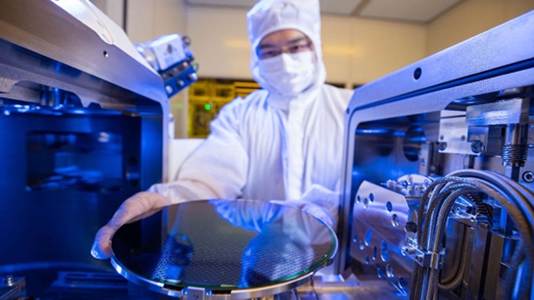
GENEVA, Switzerland, Sep 19, 2025 – STMicroelectronics is investing over $60 million in a pilot line at its Tours site in France to advance panel-level packaging (PLP) technology. Set to start operations in Q3 2026, the facility will focus on improving chip manufacturing, reducing device size, and supporting products for automotive, industrial, and consumer sectors.
PLP is an automated chip packaging and test process that uses large rectangular panels instead of circular wafers, improving manufacturing throughput, reducing costs, and enabling smaller devices for automotive, industrial, and consumer applications.
“The development of our PLP capabilities in our Tours site is aimed at advancing this innovative approach to chip packaging and test manufacturing technology, boosting efficiency and flexibility so it can be rolled out across a wide portfolio of applications, including RF, analog, power and microcontrollers. A multidisciplinary team of experts in manufacturing automation, process engineering, data science and analytics, as well as technology and product R&D, will collaborate on this program, which is a key part of a larger strategic initiative focused on heterogeneous integration – a scalable, efficient new approach to chip integration,” said Fabio Gualandris, president quality, manufacturing and technology of STMicroelectronics. “With our fab in Malta, ST has already demonstrated its capability to deliver high-performing chip packaging and test in Europe. As we reshape our global manufacturing footprint, this new initiative in Tours will expand our process, design and manufacturing innovation capabilities supporting the development of next-generation chips in Europe”.
The PLP pilot line will align with the regional R&D ecosystem, including the CERTEM center, and involves redefining roles at some sites in France and Italy to support long-term operations.
ST’s PLP technology focuses on direct copper interconnect (DCI). DCI replace the wire connections of chips with their encapsulation support. DCI provides improved performance conventional chip packaging methods that use solder bumps. This technology with direct connection without wire supports new product development by reducing power losses (such as resistance and inductance), enhancing heat dissipation and enabling miniaturization.
PLP-DCI also allows the integration of multiple chips within packages, known as System in Package (SiP).
Source: STMicroelectronics
About STMicroelectronics

STMicroelectronics, established in 1987 through the merger of Italy’s SGS Microelettronica and France’s Thomson Semiconducteurs, is a global semiconductor company headquartered in Geneva, Switzerland. The company offers a range of products, including analog chips, discrete power semiconductors, microcontrollers, and sensors, serving industries such as automotive, industrial, personal electronics, communications equipment, and computers. In 2023, STMicroelectronics reported revenues of $17.3 billion, with over 50,000 employees worldwide and offices in 40 countries. The company is committed to sustainability, aiming for carbon neutrality in scope 1 and 2 emissions, and partially scope 3, by 2027.