

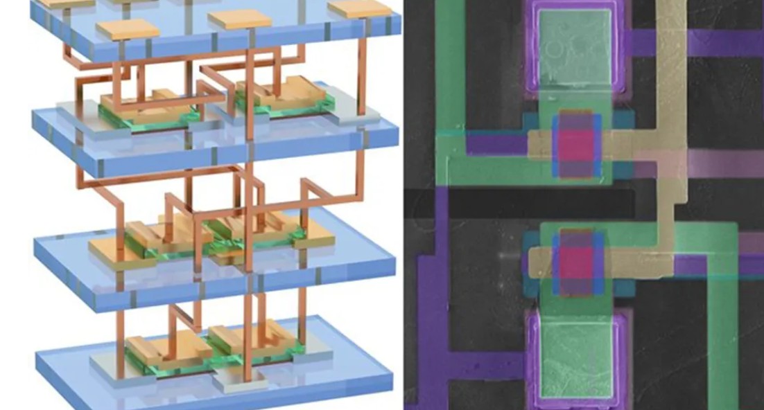
As artificial intelligence drives demand for faster and more efficient processors, researchers have developed a three-dimensional silicon chip that stacks circuits vertically instead of spreading them across a flat surface. The breakthrough addresses one of the semiconductor industry’s biggest challenges: continuing to increase computing performance as conventional two-dimensional chip designs approach their physical limits. By building circuits on top of one another, the new architecture packs more transistors into the same footprint while reducing the distance electrical signals must travel, improving both speed and energy efficiency, tells Live Science.
The research, published in Nature, introduces a manufacturing process that overcomes a longstanding obstacle to monolithic 3D chip integration. Traditionally, fabricating additional circuit layers requires high temperatures that can damage previously built components. The new approach instead uses ultrathin, single-crystal silicon membranes and a low-temperature process of approximately 200°C (392°F), allowing multiple layers to be stacked without degrading existing circuitry.
To demonstrate the concept, the researchers fabricated a prototype containing three vertically stacked silicon layers, each with 625 transistors. Although the chip is far less complex than today’s commercial processors, testing showed that the stacked architecture maintained excellent electrical performance while achieving higher current flow than previous attempts at monolithic 3D integration. The team also successfully built functional logic circuits and memory structures, demonstrating that the technology can support practical computing applications rather than serving as only a laboratory experiment.
The innovation could help extend the progress described by Moore’s Law, which has slowed as transistor miniaturization encounters quantum and manufacturing limits. Instead of making transistors continually smaller, chipmakers could increase computing density by building upward. Shorter electrical connections between layers also reduce communication delays and lower power consumption, making the approach especially attractive for AI workloads that require enormous processing capacity.
The researchers acknowledge that significant work remains before the technology reaches commercial production. The prototype must scale from hundreds to billions of transistors while maintaining high manufacturing yields and reliability. Even so, the study demonstrates that vertically integrated silicon chips can be produced without overheating, opening a promising path toward more compact, powerful, and energy-efficient processors for future AI systems, data centers, and high-performance computing applications.
