

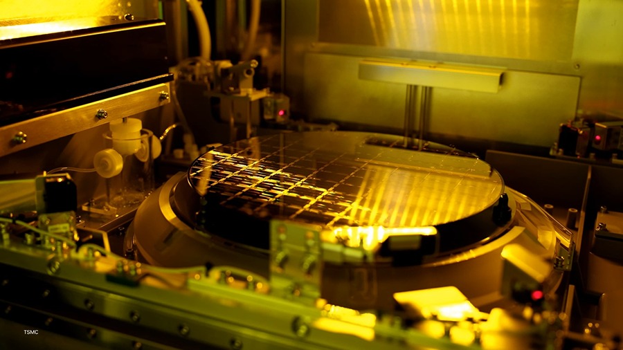
TAIPEI, Taiwan (NVIDIA GTC), June 12, 2026 – TSMC is using NVIDIA accelerated computing and AI in advanced-node semiconductor design and manufacturing workflows to reduce turnaround time, improve energy efficiency, increase yield and raise fab productivity.
The work spans semiconductor design transfer, transistor modeling, process control, lithography, defect inspection and fab operations. TSMC is applying NVIDIA GPUs, CUDA-X libraries, AI models, NVIDIA Metropolis, NVIDIA TAO Toolkit and NVIDIA Omniverse libraries across stages of the chip manufacturing lifecycle.
“NVIDIA and TSMC have worked together for nearly three decades to push the limits of computing,” said Jensen Huang, founder and CEO of NVIDIA. “TSMC is bringing NVIDIA AI and accelerated computing into the fab itself, tackling some of the world’s most complex design and manufacturing challenges with simulation, optimization and AI to improve speed, efficiency and yield for the next generation of chips.”
“TSMC and NVIDIA have built a long-standing partnership rooted in advancing the technologies that make the next generation of computing possible,” said C.C. Wei, chairman and CEO of TSMC. “By using NVIDIA accelerated computing and AI across fab operations optimization, lithography, process control and inspection, TSMC is strengthening our technology leadership and manufacturing excellence to support our customers’ future products and success.”
NVIDIA CUDA-X Libraries for Fab Workloads
Advanced semiconductor design and manufacturing require computational workloads and fab operations across chip-design transfer, transistor modeling, process control and fab productivity.
TSMC is using NVIDIA CUDA-X libraries and AI models to accelerate these workloads on NVIDIA GPUs:
- Computational lithography: TSMC is using NVIDIA cuLitho, a GPU-accelerated library for lithography, the chip mask design printing process. The technology provides a 20–50% improvement in cost effectiveness or cycle time compared with CPU-based computational lithography while maintaining the same cost of ownership.
- Transistor, equipment and process simulation: TSMC is using NVIDIA cuEST, a GPU-accelerated electronic structure simulation library, for semiconductor material design. The library provides 50x faster chemistry simulations on average.
- Advanced process control: TSMC is using the NVIDIA cuML machine learning library to accelerate large-scale analytics on NVIDIA GPUs. The approach speeds algorithms and process thousands of parameters across thousands of steps as precision inputs for machine learning models.
- Fab operations optimization: TSMC is using CUDA-based GPU-accelerated scheduling computation on NVIDIA H200 GPUs to improve fab productivity. The system manages streamline production paths and increases fab productivity.
AI for Defect Inspection
TSMC is using the NVIDIA Metropolis platform and NVIDIA TAO Toolkit to improve defect classification. Using vision AI, TSMC has improved detection of defects at nanometer scale.
The systems also help TSMC improve quality inspection while reducing repeated labeling and retraining as process conditions, inspection tools and defect types change.
NVIDIA Omniverse to Build FabTwin
TSMC is exploring NVIDIA Omniverse libraries to build FabTwin, a virtual fab environment for evaluating process tool layouts and related simulation workflows. By testing design scenarios digitally before physical implementation, TSMC can compare complex configurations flexibly and identify potential constraints earlier, improving planning efficiency and supporting decisions before physical or capital commitments are made.
Source: NVIDIA
About NVIDIA

NVIDIA, founded in 1993 and headquartered in Santa Clara, CA, designs and manufactures graphics processing units, systems on chips, networking hardware, and AI intelligence software such as CUDA. Its products serve industries including gaming, data centers, autonomous vehicles, professional visualization, robotics, health care, and energy. The company introduced the GPU in 1999 and later expanded into accelerated computing and AI infrastructure. In gaming, its GPUs support high-performance rendering, while in AI and high-performance computing, its systems provide the infrastructure for training and deploying large-scale models. NVIDIA also develops tools for robotics and autonomous driving.
About TSMC

Taiwan Semiconductor Manufacturing Co. (TSMC) is a semiconductor foundry based in Hsinchu, Taiwan. Founded in 1987, the company manufactures chips for customers that design but do not produce semiconductors in their own fabs. TSMC produces semiconductor components using process technologies that include 5-nanometer and 3-nanometer nodes, with 2-nanometer production planned. Its customers serve consumer electronics, computing, automotive, networking and industrial markets. Technology companies use TSMC manufacturing capacity for chips used in smartphones, data centers, AI systems and autonomous vehicles. TSMC employs about 84,000 people worldwide. The company served 530 customers and manufactured about 12,000 products for various applications.
