

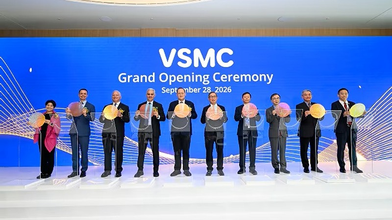
Singapore, Sep 29, 2026 – VisionPower Semiconductor Manufacturing Company (VSMC) has begun risk production at its first 12-inch (300mm) fab in Tampines, Singapore. The facility will support 130nm to 40nm processes, with volume production scheduled for Q1, 2027.
VSMC reports yield above 99% for the fab’s first sample lot following 22 months of construction. The fab will support mixed-signal, power management, analog and interposer applications for high-performance computing (HPC), mobile, automotive, industrial and consumer markets.
VSMC expects the fab to reach full capacity in 2029, producing approximately 44,000 300mm wafers monthly. The project is expected to create about 1,600 jobs.
The opening ceremony was attended by Singapore’s Minister for Trade and Industry (Energy and Industry), Dr. Tan See Leng; Economic Development Board (EDB) chairman Mr. Png Cheong Boon; and JTC Corporation CEO Ms. Jacqueline Poh. Representatives from TSMC, customers, suppliers, industry associations and government agencies also attended.
Leuh Fang, VSMC and VIS chairman said: “Today’s opening ceremony marks a significant milestone for VSMC and reflects VIS’ long-term commitment to deepening its presence in Singapore while expanding its global footprint. Since establishing the joint venture in 2024, we have worked closely with NXP Semiconductors and our partners to complete construction of our first 12-inch fab. With the fab now officially operational, we will be better positioned to meet our customers’ growing demand for specialty IC manufacturing, further strengthen the resilience of the global semiconductor supply chain, and contribute to the continued growth of Singapore’s high-tech industry and semiconductor ecosystem.”
Rafael Sotomayor, president and chief executive officer of NXP Semiconductors added: “The VSMC joint venture fab marks an important milestone in further strengthening NXP’s manufacturing base and assurance to support long-term customer demand. Building on decades of operations and investment in Singapore, VSMC enhances our geographic resilience, supply control, and cost competitiveness, while advancing our differentiated hybrid manufacturing strategy. Our planned manufacturing capacity at VSMC remains unchanged, helping us drive sustainable growth and deliver the innovative technologies that are enabling the next generation of intelligent edge and Physical AI systems.”
Ms. Cindy Koh, executive vice president, Singapore Economic Development Board (EDB) continued: “VSMC’s fab reflects the strong confidence that global companies continue to place in Singapore as a global node for advanced manufacturing and semiconductor value chain. Beyond adding new capabilities and capacity to Singapore’s semiconductor ecosystem, VSMC’s collaborations with our institutes of higher learning will equip our local workforce to contribute to technologies that shape industries and trends. VSMC’s efforts across carbon abatement, energy efficiency and water recycling reflects its ongoing commitment to more sustainable manufacturing practices in Singapore.”
VSMC constructed the fab in accordance with Leadership in Energy and Environmental Design (LEED) and Singapore’s Green Mark standards. The facility incorporates renewable energy measures.
VSMC has also signed memorandums of understanding (MoUs) with universities in Singapore for semiconductor workforce development. Its training activities include internships and professional training programs.
Source: VSMC
About VSMC

VisionPower Semiconductor Manufacturing Co. (VSMC), established in 2024, is a specialty chip foundry headquartered in Singapore. It is a joint venture between Vanguard International Semiconductor and NXP Semiconductors. Its planned 300-millimeter wafer fab in Tampines is scheduled to begin production in 2027. VSMC offers multi-project wafer prototyping, mask preparation and production, storage, design consultation and verification support. Its process technologies include 130-nanometer bipolar-CMOS-DMOS, 40-nanometer ultra-low-power and embedded-flash processes. These support chips for automotive, industrial, consumer, mobile, computing, communications and IoT applications. The company plans to use automated material handling, AI-based quality management and energy-efficient manufacturing at its Singapore facility. The fab is expected to produce 55,000 wafers monthly by 2029.
