

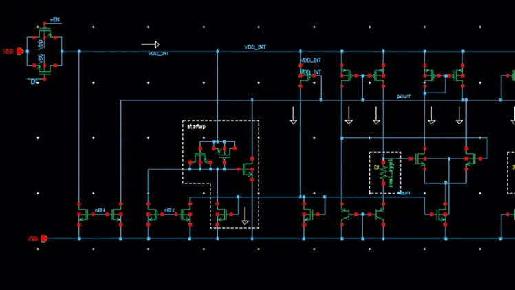
TESSENDERLO, Belgium, May 29, 2026 – X-FAB and Cadence are extending their semiconductor design collaboration to address node migration, a recurring task for chip teams moving designs between manufacturing processes. The companies are combining X-FAB process design kits with Cadence Virtuoso Studio design migration technology to automate transitions across semiconductor process nodes.
The workflow gives X-FAB customers a method for moving designs between technology nodes. Cadence Virtuoso Studio supports the process with built-in functions to support right-first-time results. X-FAB said a proof of concept demonstrated migration from 180 nm to 110 nm, with the broader offer supporting a range from 1 µm to 110 nm.
The approach connects the Cadence migration environment with X-FAB’s PDKs (Process Design Kit). While Cadence provides the design migration framework and circuit re-optimization tools, X-FAB contributes process knowledge and device mapping expertise. Customers receive dedicated mapping files to translate devices between technologies, reduce migration complexity and preserve critical performance parameters.
“With the PDK support of Cadence Virtuoso Studio design migration, we enable our customers to transition smoothly between technologies,” said Melanie Wilhelm, design technology manager at X-FAB. “The approach allows us to deliver a highly efficient and reliable migration path. The X-FAB engineering team is committed to providing this level of support, helping customers stay agile and responsive in an increasingly demanding market landscape.”
“Design migration is becoming a strategic priority for semiconductor companies navigating technology evolution, supply chain issues, and geopolitical challenges,” said Ashutosh Mauskar, corporate vice president of custom products group at Cadence. “Our continued collaboration with X-FAB reflects a shared commitment to delivering robust, scalable solutions that simplify migration and support our customers’ long-term innovation roadmaps.”
The work targets CMOS developers that need to reuse designs across process nodes. The automation combines Cadence migration tools with X-FAB technologies to reduce migration time, support design performance and maintain continuity across node transitions.
Source: X-FAB
About X-FAB

X-FAB is a specialty semiconductor foundry headquartered in Tessenderlo-Ham, Belgium. Founded in 1992, the company manufactures wafers for analog and mixed-signal semiconductor devices and provides design support and process technologies for customer chip development. Its work covers integrated circuits, MEMS, microsystems, photonics devices, silicon carbide devices and gallium nitride devices. X-FAB offers CMOS, SOI, photonics, microfluidics, sensor and high-voltage semiconductor processes. The company serves fabless semiconductor companies, original equipment manufacturers and integrated device manufacturers. Its customer industries include automotive, industrial and medical markets, with additional work in communications and consumer applications. X-FAB operates six wafer fabs in Germany, France, Malaysia and the United States. The company reported more than 400 customers worldwide.
About Cadence

Cadence Design Systems is a U.S.-based technology firm that develops electronic design automation (EDA) tools, hardware, and IP for designing integrated circuits and electronic systems. Formed in 1988 through the merger of SDA Systems and ECAD, the company is headquartered in San Jose, CA. Cadence provides software and solutions for designing SoCs, PCBs, and complete electronic systems used in the semiconductor, automotive, aerospace and defense, telecommunications, and consumer electronics industries. Its tools support both digital and analog design workflows. Cadence employs about 12,000 people globally.
