This IEEE Spectrum article explains that a major push is underway in Austin, Texas, to convert an older semiconductor fabrication facility into the world’s first dedicated foundry for 3D heterogeneous integration (3DHI), the stacking of chips made from multiple materials, not just silicon.
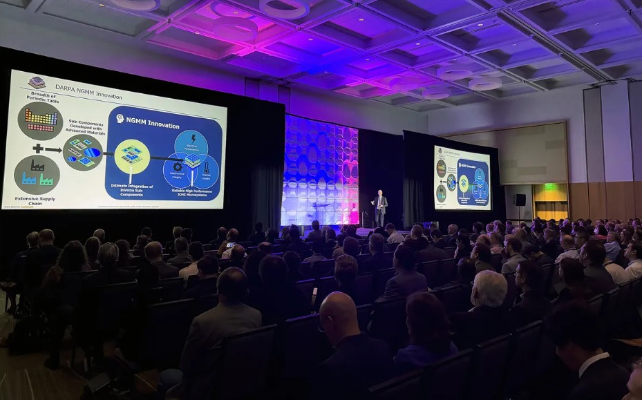
Under the Texas Institute for Electronics (TIE) initiative, backed by DARPA’s Next-Generation Microelectronics Manufacturing (NGMM) program, the goal is to go beyond traditional 3D stacking of silicon dies (which might yield ~30× performance gains) to stacking dissimilar materials, such as silicon, gallium-nitride, silicon-carbide, and others, to reach potential ~100× improvements.
The facility has received $552 million from Texas plus $840 million from DARPA and is set to install state-of-the-art tooling by Q1 2026, laying the groundwork for a self-sustaining business post-mission.
A central challenge: merging chips made from different materials, each with distinct thermal expansion, mechanical behavior, and sizes, into micrometer-precision stacks with reliable interconnects and high yield. TIE engineers are now developing process design kits (PDKs) and assembly-design kits (ADKs) to formalize rules for 3D assembly.
TIE’s initial exemplar projects include a phased-array radar, an infrared imager (focal-plane array), and a compact power converter, each illustrating how heterogeneous chip stacks can unlock new capabilities.
This foundry model signals a shift: advanced packaging isn’t merely a stop-gap for Moore’s Law, it’s becoming the platform for radical system-level gains. Performance, power, and form-factor all benefit when logic, memory, and novel materials can be stacked in unified architectures. Still, manufacturing maturity, yield management, thermal control, and supply-chain readiness remain key obstacles.
This article outlines the bold attempt to turn 3D heterogeneous integration from a lab concept into industrial-scale manufacturing, across diverse materials and application domains.