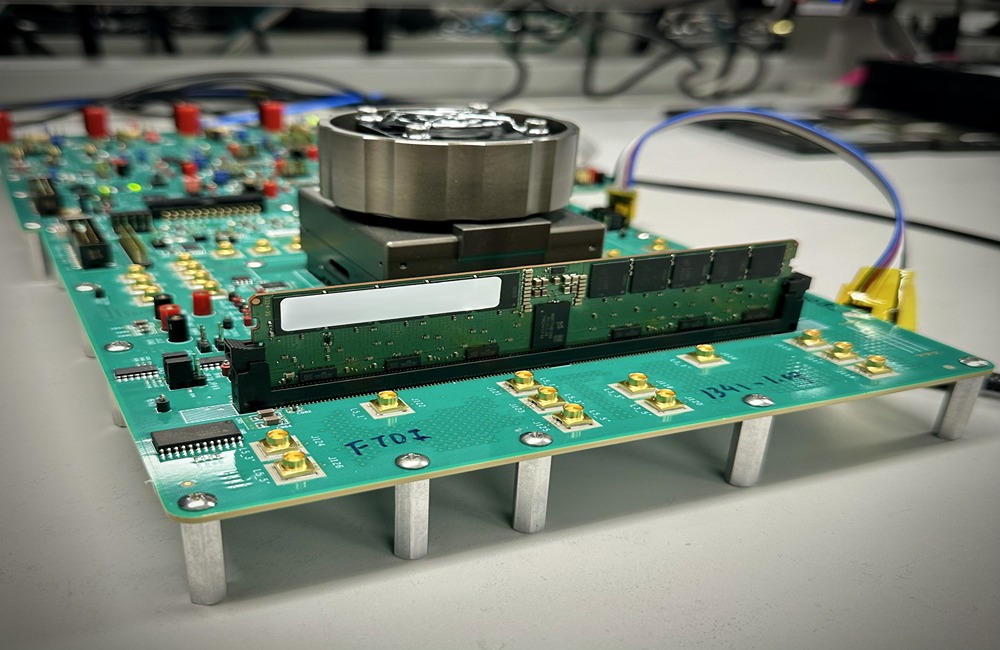
SAN JOSE, CA, Apr 24, 2025 – Cadence has introduced a DDR5 12.8Gbps MRDIMM Gen2 memory IP system solution on the TSMC N3 process, claimed to be the industry’s first. The solution supports higher memory bandwidth for AI workloads in enterprise and cloud data center applications. The Cadence DDR5 MRDIMM IP is built on a scalable architecture based on the company’s DDR5 and GDDR6 product lines. It is currently used in projects with AI, HPC, and data center customers.
The Cadence DDR5 IP includes a PHY and a controller as a complete memory subsystem. The design is validated in hardware using MRDIMMs (Gen2), reaching a 12.8 Gbps data rate that doubles the bandwidth using DDR5 6400 Mbps DRAM parts. The DDR5 IP memory subsystem is based on Cadence’s silicon-proven architecture, ultra-low latency encryption, and RAS features. The DDR5 MRDIMM Gen2 IP is designed to enable advanced SoCs and chiplets with flexible floorplan design options. The architecture allows fine-tuning of power and performance to meet specific application needs.
“The Cadence DDR5 IP portfolio, together with Micron’s industry-leading 1γ (1-gamma)-based DRAM, meets the increasing demand for higher memory bandwidth, density and reliability for AI processing workloads. These memory enhancements are pivotal in enabling the next generation AI/ML and HPC applications in data center and enterprise environments,” said Praveen Vaidyanathan, vice president and general manager of Micron’s data center products.
“Cadence’s DDR5 MRDIMM IP system solution, paired with MRDIMM modules featuring Montage’s memory buffers, delivers a high-performance memory subsystem for next-generation servers with doubled bandwidth,” said Stephen Tai, president at Montage Technology. “Montage’s MRCD02/MDB02 chips for MRDIMMs, capable of blazing 12.8Gbps data rates, are ready to enable server and data center products.”
“Data center and enterprise applications stand to gain a significant performance advantage from Cadence’s DDR5 12.8Gbps MRDIMM IP system solution, as evidenced by large customers turning to Cadence to deliver this innovative technology,” said Boyd Phelps, senior vice president and general manager of the Silicon Solutions Group at Cadence. “This new leading-edge memory IP system both raises the bar and establishes a roadmap that future-proofs our customers’ next-generation SoC and chiplet products for generations to come.”
Cadence’s DDR5 controller and PHY have been verified with Cadence’s Verification IP (VIP) for DDR to enable rapid IP and SoC verification closure. Cadence VIP for DDR5 includes a solution from IP to system-level verification with DFI VIP, DDR5 memory model, and System Performance Analyzer.
Source: Cadence
About Cadence
![]()
Cadence Design Systems, Inc. is a U.S.-based technology company specializing in electronic design automation (EDA) software, hardware, and intellectual property (IP) solutions. Founded in 1988 through the merger of SDA Systems and ECAD, Cadence is headquartered in San Jose, CA. The company serves industries such as semiconductors, automotive, aerospace and defense, consumer electronics, and telecommunications. Cadence’s offerings include tools for designing integrated circuits, systems on chips (SoCs), printed circuit boards (PCBs), and complete electronic systems. As of 2024, Cadence reported annual revenue of approximately $4.64 billion and employed around 12,703 people worldwide. The company’s comprehensive solutions support the development of advanced electronic products across various sectors.