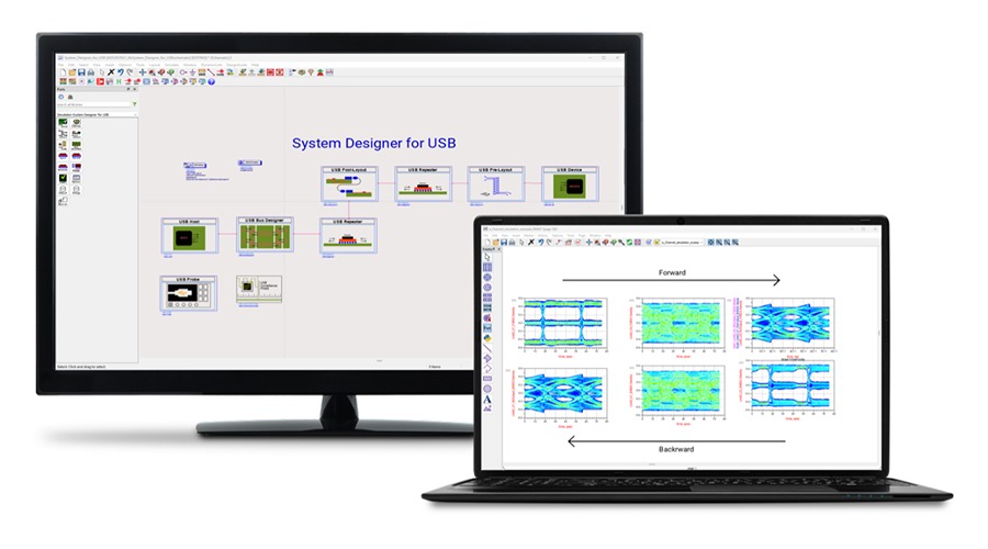
SANTA ROSA, CA, May 13, 2025 – Keysight Technologies, Inc. has announced the launch of System Designer for USB, its latest solution for high-speed digital USB (Universal Serial Bus) design for personal computers, mobile devices, and edge AI applications. System Designer for USB enables comprehensive modeling and simulating of systems adhering to the USB4 standard. This system-level approach enables validation and speeds up product release.
As data demands increase across personal computers and mobile devices, maintaining high-speed data transfer and signal integrity over USB interfaces is critical – especially for bandwidth-heavy applications. To address this, the industry has adopted the USB4 specification, which delivers data rates up to 120Gbps using PAM3 (three-level pulse-amplitude modulation), while maintaining compatibility with the existing USB-C connector standard. By designing with these next-gen USB protocols and verifying for USB4 compliance, hardware engineers can reduce the likelihood of design re-spins, control development costs, and improve time-to-market for new products.
Key Benefits of the System Designer for USB:
- System Designer for USB streamlines the setup of complex USB systems, including multi-link, multi-lane, and multi-level (PAM3) configurations through a smart design environment. It simplifies simulation setup and reduces time-to-first-insight.
- The USB Algorithmic Modeling Interface (AMI) modeler, which supports Non-Return to Zero (NRZ) and PAM3 modulations, enables the implementation of efficient USB systems.
- The integrated simulation-driven compliance test solution helps reduce design costs by minimizing design iterations and shortening time-to-market.
Hee-Soo Lee, High-Speed Digital Segment Lead, Keysight EDA, said: “We continue to expand our standards-driven workflow approach to support our customers. Our high-speed digital product portfolio is leading the EDA industry with the most accurate and advanced simulation software for signal integrity analysis and compliance test validation. Digital standards are critical to the performance of electronic systems. Designers using our System Designer for USB simulation solutions in their workflows can shift left their development cycle to save significant time and cost.”
Source: Keysight Technologies
About Keysight Technologies

Keysight Technologies, established in 2014 as a spin-off from Agilent Technologies, is a leading provider of electronic design and test solutions. Headquartered in Santa Rosa, California, the company offers a portfolio of hardware and software products, including oscilloscopes, signal generators, and electronic design automation (EDA) software. The solutions serve industries, such as telecommunications, aerospace and defense, automotive, energy, semiconductor, and general electronics. As of 2024, Keysight employs approximately 15,500 people and reported annual revenue of $5.0 billion. The company’s global presence spans the Americas, Europe, and Asia Pacific, supporting over 30,000 customers in more than 100 countries. Keysight is known for driving innovation, with over 3,800 patents and a focus on research and development.