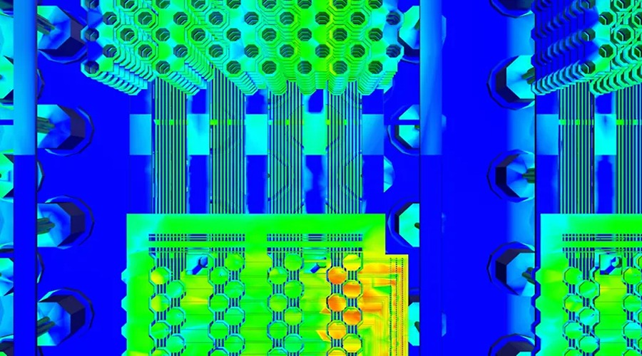
PITTSBURGH, PA, Apr 30, 2025 – Ansys has announced thermal and multiphysics signoff tool certifications for designs manufactured with Intel 18A process technology. The certifications confirm the functionality and reliability of semiconductor systems used in applications like AI chips, graphics processing units (GPUs), and high-performance computing (HPC) products. Intel Foundry and Ansys have also introduced a multiphysics signoff analysis flow for Intel Foundry’s EMIB technology, which is used to create multi-die 3D integrated circuit (3D-IC) systems.
RedHawk-SC and Totem deliver speed, accuracy, and capacity to analyze power integrity and reliability of Intel 18A RibbonFET Gate-All-Around (GAA) transistors with PowerVia backside power delivery. Ansys is introducing HFSS-IC Pro, an addition to the HFSS-IC product family, for scalable electromagnetic analysis. HFSS-IC Pro is certified for modeling on-chip electromagnetic integrity in radio frequency chips, WiFi, 5G/6G, and other telecommunication applications built on the Intel 18A process node.
EMIB supports 3D-IC for high-performance microprocessors and heterogeneous integrated systems. It connects different chip types to improve the integration and function of advanced computing systems. The flow includes thermal reliability analysis with RedHawk-SC Electrothermal. Ansys and Intel Foundry are expanding their collaboration to include next-generation EMIB-T technology. This technology will add through-silicon vias (TSVs) to EMIB. The EMIB-T flow is expanded to include HFSS-IC Pro and SIwave for signal integrity analysis and RedHawk-SC and Totem for power integrity analysis.
The qualification process for RedHawk-SC, Totem, and HFSS-IC Pro is under way for the Intel 18A high-performance process node (Intel 18A-P). Customers may request the latest Intel PDK to begin early design work and IP development. These solutions are part of the Intel 14A-E process definition and Design Technology Co-Optimization (DTCO).
In addition, Ansys has joined the Intel Foundry Chiplet Alliance, a part of the Intel Foundry Accelerator Alliance. This partnership supports the development of an ecosystem for designing and manufacturing compatible chiplets.
“Our approach to multi-die assembly is changing the way the industry thinks about stacking chips and designing for efficiency,” said Suk Lee, vice president & general manager, Ecosystem Technology Office at Intel Foundry. “Ansys tools are critical in this process because they help our mutual customers validate their designs with extreme accuracy – saving them costs that may not otherwise be recoverable. Furthermore, we are looking forward to Ansys’ participation in the Intel Foundry Chiplet Alliance, which is critical to advancing chiplet technology.”
“Ansys’ suite of multiphysics simulation tools instill confidence in our customers, ensuring their semiconductor systems achieve the highest levels of thermal, signal, power, and mechanical integrity,” said John Lee, vice president and general manager of the electronics, semiconductor, and optics business unit at Ansys. “While customers may adopt various methods for chip design, the need for precise tools and solutions to ensure reliability remains constant — this is where Ansys excels. By joining the Intel Foundry Chiplet Alliance and deepening our collaboration with Intel Foundry, Ansys is delivering on its commitment to providing open-source and interoperable technology in pursuit of engineering excellence.”
Source: Ansys
About Ansys

Ansys, founded in 1970, specializes in engineering simulation software. It offers a comprehensive suite of tools for structural analysis, fluid dynamics, electromagnetic field simulation, and more, enabling industries to design and test products virtually. Ansys software has enabled innovators across industries to push boundaries by using the predictive power of simulation. Serving sectors such as aerospace and defense, automotive, energy, industrial equipment, materials and chemicals, consumer products, healthcare, and construction, Ansys supports innovation across diverse fields. As of 2023, the company reported annual revenues exceeding $2.3 billion and employed over 6,200 people worldwide. Headquartered in Canonsburg, Pennsylvania, Ansys continues to advance engineering simulation technologies, empowering organizations to enhance product development processes.
About Intel Foundry

Intel Foundry, established as a standalone business unit in 2021, is Intel Corporation’s dedicated semiconductor manufacturing division headquartered in Santa Clara, California. It offers advanced silicon process technologies, including Intel 18A and the forthcoming 14A nodes, alongside cutting-edge packaging solutions like Foveros and EMIB. Serving industries such as automotive, aerospace, defense, and AI, Intel Foundry aims to become the world’s second-largest foundry by 2030. In 2023, it reported revenues of $18.9 billion but faced an operating loss of nearly $7 billion, reflecting significant investments in expanding manufacturing capabilities. The division is actively collaborating with major tech firms like Nvidia and Broadcom, who are testing chips using Intel’s 18A process, indicating growing confidence in its manufacturing advancements. With a focus on delivering comprehensive system-level solutions and a resilient global supply chain, Intel Foundry is positioning itself as a key player in the semiconductor industry.
