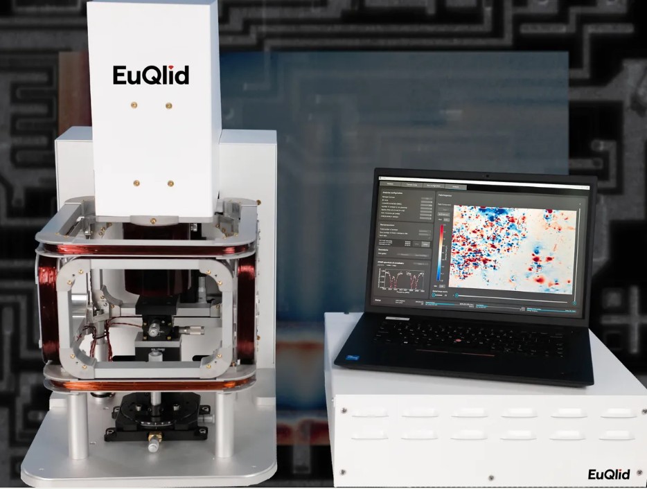
In an article from IEEE Spectrum, Charles Q. Choi profiles startup EuQlid and its quantum-sensor platform called QuMRI, designed to inspect 3D-stacked semiconductor chips for hidden flaws. The boom in stacked transistor layers has introduced new inspection challenges: conventional optical or X-ray inspections either lack depth penetration or impose damage. EuQlid’s solution uses artificial-diamond sensors with nitrogen-vacancy (NV) defects to non-invasively map current flows in buried interconnects and detect defects without harming the chip.
EuQlid claims its technology can operate up to 100–150 µm deep, aligning with industry needs for next-gen 3D stack inspection, and at speeds up to 100× faster than X-ray inspection. The process uses NV-centers in diamond, which respond to changes in magnetic and electric fields: when illuminated with green light, the fluorescent behavior of the NV center shifts in response to nearby current flows. This lets engineers visualize defects such as incomplete metal deposition, silicon cracks, or other connectivity failures beneath the surface.
For semiconductor manufacturing, the implications are significant. With stacked chips becoming more prevalent to boost performance and lower energy per computation, uncovering hidden flaws early, and without destructive inspection, is critical to yield, cost, and reliability. According to Materials and Components Research Center Imec, the QuMRI system addresses a key gap for next-gen device fabs.
Beyond defect detection, the article notes potential future uses including uncovering hardware-trojans (malicious embedded circuitry) by spotting anomalous current flows. This shift underscores a new frontier: quantum-sensing tools moving from lab to fab floor, especially where conventional inspection methods are reaching physical or cost limits.