SAN JOSE, CA, Jan 15, 2026 – Cadence has introduced a chiplet spec-to-packaged parts ecosystem to reduce engineering complexity and shorten development cycles for chiplets targeting physical AI, data center, and high-performance computing (HPC) applications. The ecosystem launches with IP partners including Arm, Arteris, eMemory, M31 Technology, Silicon Creations, Trilinear Technologies, and silicon analytics provider proteanTecs. To support adoption and reduce implementation risk, Cadence is working with Samsung Foundry to build a silicon prototype demonstration of the Cadence physical AI chiplet platform on the Samsung SF5A process.
Cadence and Arm are aligning their technologies to support chiplet-based designs for physical AI and infrastructure AI workloads. Cadence plans to integrate the Arm Zena Compute Subsystem (CSS) and supporting IP into its physical AI chiplet platform and chiplet framework. The new Cadence solutions targets edge AI use cases in automotive, robotics, and drones, while also supporting I/O and memory chiplets for data center, cloud, and HPC systems. The collaboration is intended to simplify development and provide a lower-risk path to chiplet adoption.
“Cadence’s new chiplet ecosystem represents a significant milestone in chiplet enablement,” said David Glasco, vice president of the compute solutions group at Cadence. “Multi-die and chiplet-based architectures are increasingly critical to achieving greater performance and cost efficiency amid growing design complexity. Cadence’s chiplet solutions optimize costs, provide customization flexibility and enable configurability. By combining our extensive IP and SoC design expertise with pre-integrated and pre-validated IP from our robust partner ecosystem, Cadence is accelerating the development of chiplet-based solutions and helping customers mitigate risk to quickly realize their chiplet ambitions with greater confidence.”
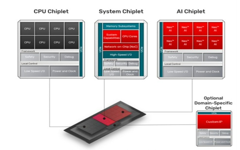
Cadence uses spec-driven automation to generate chiplet architectures that integrate Cadence IP and third-party IP with management, security, and safety functions. The EDA tool combines logic simulation with Cadence Xcelium logic simulator and emulation with the Cadence Palladium Z3 enterprise emulation platform, and feedback-driven physical design for place-and-route optimization. The chiplet architectures align with the Arm chiplet system architecture and are designed to support future OCP foundational chiplet standards. For connectivity, Cadence provides UCIe IP for die-to-die connectivity and a protocol IP portfolio that supports memory and interconnect standards including LPDDR6/5X, DDR5-MRDIMM, PCI Express (PCIe) 7.0, and HBM4.
Source: Cadence
About Cadence

Cadence Design Systems, Inc. is a U.S.-based technology firm that develops electronic design automation (EDA) tools, hardware, and IP for designing integrated circuits and electronic systems. Formed in 1988 through the merger of SDA Systems and ECAD, the company is headquartered in San Jose, CA. Cadence provides software and solutions for designing SoCs, PCBs, and complete electronic systems used in the semiconductor, automotive, aerospace and defense, telecommunications, and consumer electronics industries. Its tools support both digital and analog design workflows. As of 2024, Cadence reported annual revenue of approximately $4.64 billion and employed about 12,703 people globally. The company’s technology supports the design, verification, and optimization of complex electronics across various industries.