A new method has been developed collaboratively by UNIST and Yonsei University to fabricate intricate patterns of two-dimensional (2D) semiconductor materials directly onto substrates, without relying on harsh chemicals, high temperatures, or complex etching, tells Tech Xplore. The innovation lies in an alcohol-based solvent system, paired with a UV-curable cross-linker, which enables high-resolution circuit formation in a cleaner, gentler way.
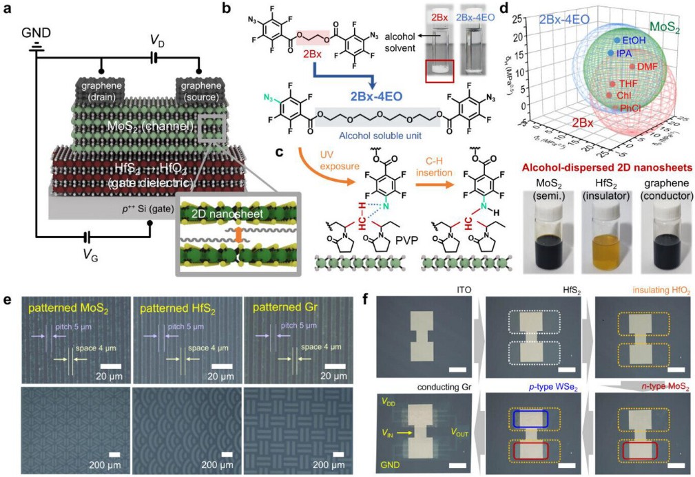
Traditional semiconductor fabrication often uses aggressive solvents, high heat, and etching that can degrade or destroy delicate 2D materials. That’s a major barrier to deploying such materials in scalable, real-world devices. In contrast, the new technique dissolves 2D nanomaterials and a custom cross-linker in isopropanol, deposits the mixture on a substrate, masks a pattern, then uses ultraviolet light to cure the cross-linker. The uncured material washes away with water, leaving behind sharp, well-defined semiconductor patterns.
The research team paid particular attention to designing the cross-linker molecules so they remain stable and soluble in alcohol, something conventional azide cross-linkers struggle with. They used Hansen solubility parameter analysis to fine-tune compatibility and dispersion of the materials.
Performance tests showed promising results. Using molybdenum disulfide (MoS₂), they fabricated transistors with a mobility of about 20.2 cm²/V·s, a threshold voltage of 2.0 V, and an on/off current ratio of 2.7 million. They also demonstrated stable operation over 60 days and built logic circuits, such as NOT, NAND, and NOR gates, and SRAM arrays combining p- and n-type semiconductors on the same substrate.
This method presents a path to scalable, eco-friendly integration of 2D materials into advanced circuits. It bridges a key gap between lab innovations and practical, high-density, low-power devices, potentially accelerating the adoption of next-generation semiconductors.