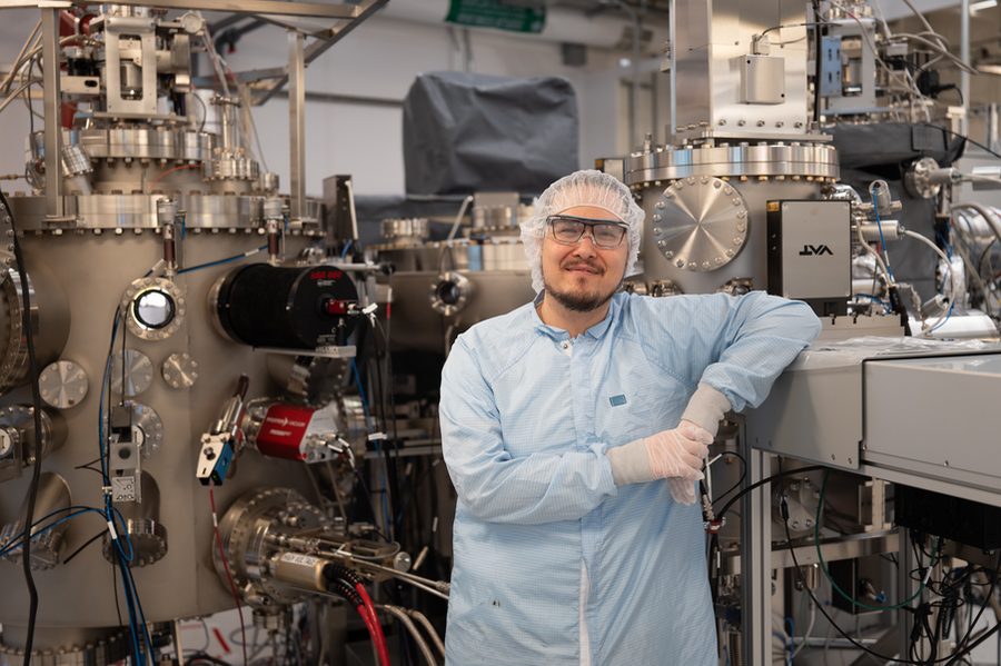
MIT has installed an advanced fabrication system designed to push quantum computing research beyond the limits of current qubit engineering. The new platform, housed inside MIT.nano’s cleanroom facilities, is a custom-built molecular beam epitaxy system, or MBE, capable of producing exceptionally pure thin-film materials under ultra-high vacuum conditions. According to MIT News, researchers see the installation as a critical step toward solving some of the deepest materials challenges facing quantum computing.
Quantum computers rely on qubits, fragile quantum states that are extremely sensitive to environmental disturbances. Over the past decade, improvements in superconducting qubits have largely come from better circuit designs that reduce sensitivity to external noise. However, researchers now believe many remaining performance limitations originate at the material level itself. Tiny defects, contamination, and structural irregularities in thin-film materials can introduce quantum noise that destabilizes qubits and increases error rates.
The new MBE system is designed to address those problems directly. Molecular beam epitaxy allows scientists to grow crystalline layers atom by atom with extraordinary precision. The multi-chamber system can deposit, process, and analyze 200-millimeter wafers while maintaining ultra-clean environments that minimize contamination. Researchers describe the setup as a “materials scientist’s playground” because it combines deposition, etching, and characterization capabilities within a tightly controlled fabrication workflow.
William D. Oliver, professor of electrical engineering, computer science, and physics at MIT, explained that future breakthroughs in quantum computing will depend increasingly on materials science and fabrication engineering rather than circuit geometry alone. By enabling researchers to systematically study the microscopic origins of noise and defects, the system may help improve qubit reliability, scalability, and manufacturing consistency.
The installation also reflects a broader shift in quantum technology research. As experimental quantum devices become more sophisticated, attention is moving from proof-of-concept demonstrations toward industrial-scale fabrication techniques resembling semiconductor manufacturing. Researchers aim not only to build more stable qubits but also to develop repeatable production methods capable of supporting large-scale quantum processors.
The project positions MIT.nano as a central hub for advanced quantum materials research, bringing together physicists, materials scientists, and engineers to explore the next generation of quantum hardware. By focusing on the atomic foundations of qubit performance, the facility represents a growing recognition that the future of quantum computing may ultimately depend as much on materials engineering as on quantum algorithms themselves.