MIT researchers have developed a fabrication method that dramatically shrinks three-dimensional structures into nanoscale photonic devices capable of manipulating visible light, potentially opening new directions for optical computing and high-speed information processing. The technique, described in a report from MIT News, enables the creation of structures with feature sizes smaller than 100 nanometers, a critical threshold for controlling visible light wavelengths.
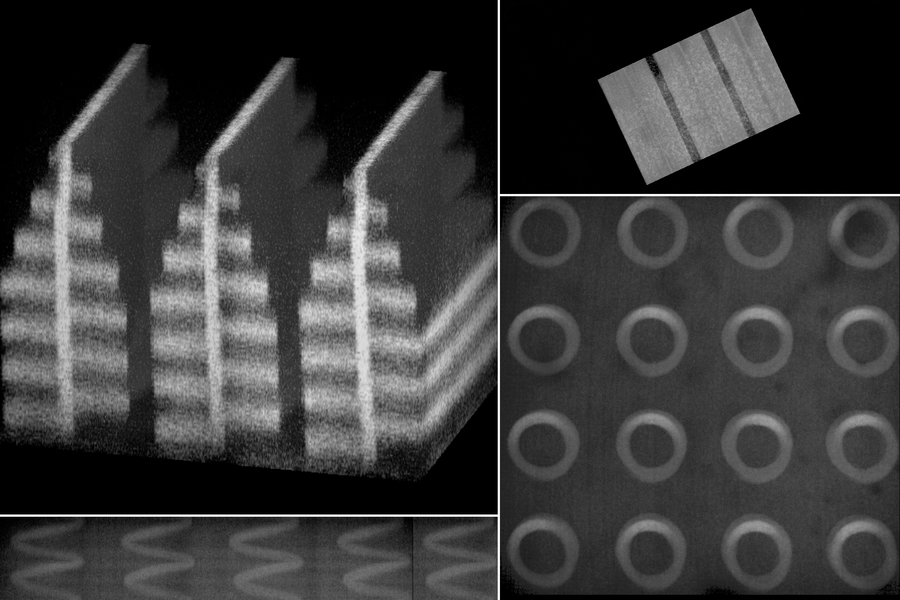
The research centers on a process called “implosion carving,” an extension of earlier work from MIT’s Boyden Lab on implosion fabrication. Researchers begin by patterning features into a hydrogel using laser-based photopatterning techniques. Tiny vacancies are then created at precise locations inside the material. After fabrication, the hydrogel is chemically processed and shrunk to roughly less than 100 nanometers of its original volume, compressing the structures into highly detailed nanoscale forms.
This shrinking process allows engineers to overcome one of the major limitations in current photonic manufacturing. Existing approaches such as two-photon lithography can create 3D nanoscale structures but struggle to achieve the sub-100-nanometer precision needed to manipulate visible light effectively. Electron-beam lithography can achieve smaller features but is generally limited to flat, two-dimensional surfaces. Implosion carving combines nanoscale precision with fully three-dimensional geometries.
Using the technique, the researchers fabricated a variety of photonic structures, including helices and shapes inspired by butterfly wings. They also demonstrated a simple photonic device capable of performing digit-classification tasks by directing and diffracting light through nanoscale patterns. The work suggests that future optical systems could process information using light instead of electricity, potentially improving speed and energy efficiency compared with conventional semiconductor technologies.
The researchers believe the approach could support applications beyond optical computing, including advanced imaging systems, nanofluidic devices, and high-throughput biological sensing. Because the process relies on shrinking larger patterned structures rather than directly manufacturing at nanoscale dimensions, it may also offer a more scalable and cost-effective route for producing complex photonic architectures.
The study reflects a broader push toward photonic computing technologies designed to handle growing computational demands while reducing energy consumption in next-generation computing systems.