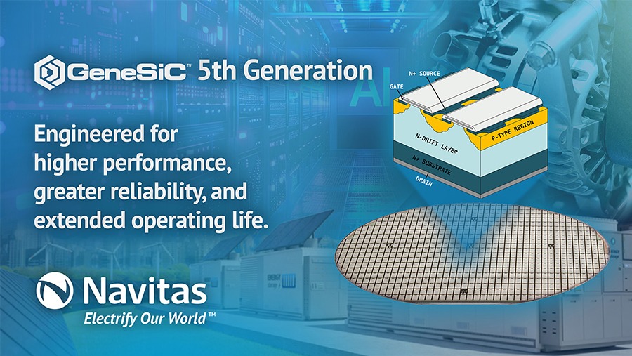
TORRANCE, CA, Feb 17, 2026 – Navitas Semiconductor has introduced its 5th-generation GeneSiC technology platform, expanding its silicon carbide power portfolio. The new High Voltage (HV) SiC Trench-Assisted Planar (TAP) MOSFET technology launches a 1200V line of MOSFETs for high-performance power conversion. It builds on the 4th generation GeneSiC platform, which includes 2300 V and 3300 V voltage devices. The move strengthens Navitas’ position in AI data centers, grid infrastructure, and industrial electrification.
Navitas’ 5th-generation MOSFET platform centers on its TAP architecture. It combines planar gate ruggedness with trench-enabled performance in the source region. The design boosts efficiency and strengthens reliability in high-voltage power electronics systems.
Navitas reports a 35% improvement in RDS,ON × QGD figure of merit (FoM) over its prior 1200 V technology. The improvement cuts switching losses, reduces heat, and supports higher switching frequencies in power electronics systems.
Navitas reports about a 25% improvement in the QGD / QGS ratio to enable high-speed switching. Combined with a stable threshold voltage (VGS,TH ≥ 3V), the platform prevents parasitic turn-on and maintains stable gate drive operation in high-noise power environments.
The 5th-generation technology improves switching performance by refining the RDS(ON) × EOSS profile and integrating a “Soft Body-Diode” structure. The changes reduce electromagnetic interference (EMI) and stabilize commutation during operation.
AEC-Plus grade qualification ensures stability and durability for AI data centers, energy and grid infrastructure applications.
Key reliability benchmarks include:
- Extended stress testing: 3x longer duration for static high-temperature, high-voltage testing (HTRB, HTGB, and HTGB-R).
- Advanced switching reliability testing: Dynamic reverse bias (DRB) and dynamic gate switching (DGS) to represent fast-switching application mission-profiles
- Industry-leading stability: Lowest VGS,TH shift over switching stress periods for long-term efficiency
- Extreme gate oxide reliability: Extrapolated gate-oxide failure time exceeding 1 million years at operating VGS at 18V and 175°C.
- Enhanced cosmic ray resilience: Low FIT (Failure In Time) rates, ensuring reliability in high-altitude and high-uptime environments.
“Our customers are redefining the boundaries of power conversion in AI data centers and energy infrastructure, and Navitas is marching along with them in every step of the way,” said Paul Wheeler, VP & GM of Navitas’ SiC business unit. He added, “significant technological improvements in our 5th generation GeneSiC technology underscore Navitas’ commitment to delivering industry-leading performance and reliability in silicon carbide MOSFETs.”
Source: Navitas
About Navitas

Navitas Semiconductor, founded in 2014 and headquartered in Torrance, CA, designs and manufactures power semiconductors based on gallium nitride (GaN) and silicon carbide (SiC) technologies. Operating under the GaNFast and GeneSiC brands, the company develops integrated GaN power ICs and SiC devices for use in applications such as AI data centers, electric vehicles, renewable energy, energy storage, industrial systems, and consumer electronics. The company employs approximately 280 people. GaNFast ICs combine power switching with control, sensing, and protection features, while GeneSiC devices target high-voltage and high-reliability applications. Navitas holds over 300 issued or pending patents and offers a 20-year warranty on its GaNFast products. It is also recognized as the first semiconductor company to achieve CarbonNeutral certification.