

As the semiconductor industry continues to pack more transistors onto microchips, one of the biggest performance bottlenecks is no longer the transistors themselves but the tiny copper interconnects that carry electrical signals between them. While copper has long been the material of choice because of its excellent conductivity, its performance deteriorates as interconnects shrink to the nanoscale. Electrons increasingly scatter from surfaces and grain boundaries, raising electrical resistance and limiting further chip scaling. Cornell University researchers have now demonstrated a promising alternative that could overcome this challenge.
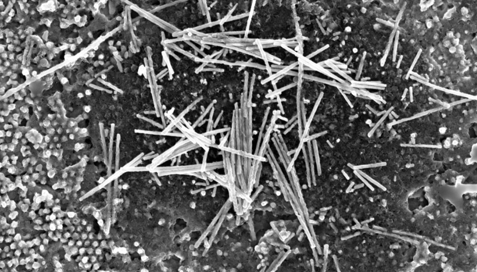
The team developed single-crystal nanowires made from niobium arsenide, a topological semimetal whose electrical behavior differs fundamentally from that of conventional metals. Unlike copper, niobium arsenide supports highly mobile surface electrons that travel with minimal scattering. As the nanowires become thinner, these protected surface states contribute more strongly to electrical conduction, producing the unusual result that conductivity actually improves with decreasing size. The material also remains stable and highly conductive at room temperature, an important advantage for practical electronic devices.
A key part of the research was the fabrication process. Instead of relying on traditional nanowire growth techniques, which offer limited control over dimensions and shape, the researchers employed thermomechanical nanomolding. The method presses bulk material into nanoscale porous molds at high temperature, producing high-quality single-crystal nanowires with diameters as small as about 10 nanometers. The process is both highly controllable and significantly faster, allowing researchers to evaluate many more candidate materials than before.
Although niobium arsenide is unlikely to replace copper directly because arsenic-containing compounds present toxicity concerns, the researchers view the work as an important proof of concept. It demonstrates that topological semimetals can offer practical engineering advantages rather than remaining purely theoretical materials. The study also establishes thermomechanical nanomolding as a powerful platform for rapidly screening new quantum materials that could enable faster, more energy-efficient microchips as conventional copper interconnects approach their physical limits.
