TOKYO, Japan and SAN FRANCISCO, CA, Feb 20, 2026 – Renesas Electronics unveiled three new system-on-chip (SoC) technologies designed for automotive multi-domain electronic control units (ECUs) and electrical/electronic (E/E) architecture. The devices integrate AI processing and chiplet functions to address rising vehicle compute demands. The SoCs are positioned as a core platform for centralized automotive control systems. Renesas presented the technologies at the International Solid-State Circuits Conference 2026 (ISSCC 2026), held Feb 15–19 in San Francisco, CA.
As automotive SoCs grow in size and complexity, centralized vehicle architectures increase design constraints. Each device must support multiple applications while meeting functional safety and automotive-grade quality requirements. Chiplets enable compute scaling but introduce added integration complexity. Processing performance also increases power consumption. Designers must address power efficiency and system safety as performance demands rise.
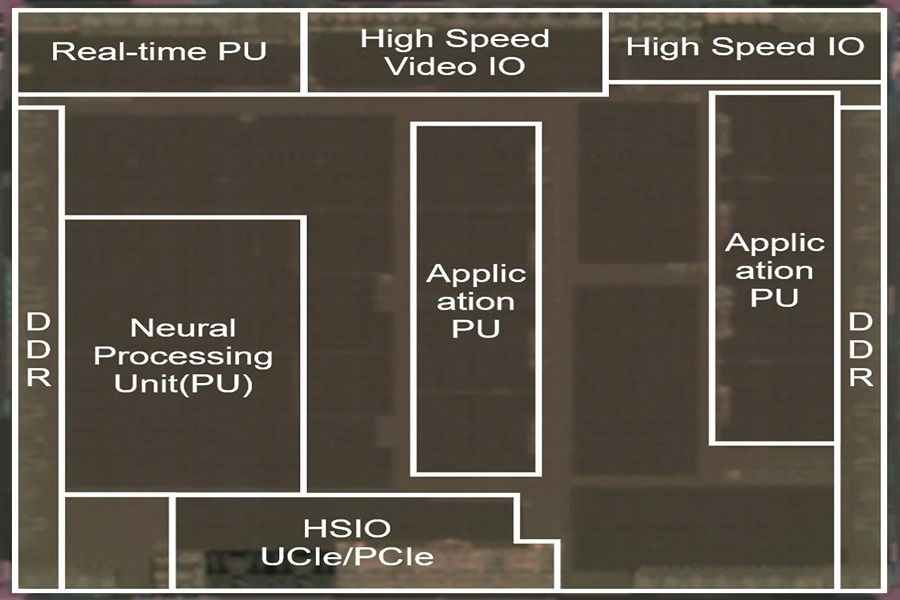
To meet these needs, Renesas has developed the below technologies:
Chiplet Architecture that Supports Functional Safety
Renesas introduced a proprietary architecture to support ASIL D compliance in chiplet-based automotive SoCs. The design combines the standard UCIe die-to-die interface with a RegionID mechanism that prevents hardware resource interference when multiple applications run at the same time, achieving Freedom from Interference (FFI).
Because conventional UCIe links do not transmit RegionIDs between dies, Renesas created a mapping method that embeds RegionIDs into physical address space and encodes them for transfer. The approach enables controlled access through the memory management unit (MMU) and real-time cores across chiplets. Testing confirmed 51.2 GB/s data transfer, near intra-SoC bandwidth limits.
Advanced AI Processing Capabilities and Automotive-Grade Quality
Renesas redesigned clock architecture in its 3 nm SoC to address neural processing unit (NPU) size and clock latency in SDV systems. NPUs have grown about 1.5 times larger than previous generations, increasing delay between shared clock sources and circuit blocks. To reduce latency and meet timing requirements, Renesas split module-level clock pulse generators into sub-module mini-CPGs while maintaining automotive-grade quality.
The multi-layer mCPG structure introduced test clock synchronization challenges tied to zero-defect automotive targets. Renesas integrated test circuits into a hierarchical CPG architecture and unified user and test clock signal paths. In test mode, the design synchronizes upper- and lower-level mCPGs under a single clock source, enabling consistent phase control. The approach supports large-scale automotive SoCs aligned with zero-defect quality expectations for SDV systems.
Advanced Power Control and Monitoring for Improved Power Efficiency and Safety
Renesas deployed advanced power gating across more than 90 power domains to control performance and energy use in automotive SoCs. The design supports power levels ranging from milliwatts to tens of watts. To reduce IR drops (voltage drops), Renesas split power switches (PSWs) into ring PSWs and row PSWs. The ring PSW limits inrush current during power-on, and the row PSW balances impedance within each domain, reducing IR drops by about 13% compared with conventional designs.
For ASIL D functional safety, Renesas implemented a dual core lock step (DCLS) configuration with independent power switches and controllers for master and checker cores. Lockstep operation detects faults if one core fails. Each PSW uses loopback monitoring to verify OFF states during failures. A temperature-resistant digital voltage meter (DVMON) monitors voltage and improves aging tolerance by 1.4 mV, reinforcing power efficiency and safety in automotive SoCs.
These new technologies are used in Renesas’ R-Car X5H SoC for automotive ECUs. With R-Car X5H, users can advance SDVs while ensuring safety and supporting autonomous driving and digital cockpit functions.
Source: Renesas Electronics
About Renesas Electronics

Renesas Electronics, based in Tokyo, supplies power management integrated circuits (PMICs) and ships more than 1.5 billion power devices annually for computing, industrial, IoT, data center, and communications markets. Its portfolio includes PMICs, discrete devices, GaN power products, and design tools such as PowerCompass and PowerNavigator. These work with microcontrollers, SoCs, and connectivity solutions to support system design. The company was formed in 2010 through the merger of Renesas Technology and NEC Electronics, with origins in semiconductor units of Hitachi, Mitsubishi, and NEC.