PLANO, TX, Apr 24, 2026 – Siemens is collaborating with TSMC to advance AI-driven automation and semiconductor design across EDA workflows. The collaboration extends Siemens’ support across the EDA workflow, including automated correction of design rule violations and certified tools for leading-edge process technologies.
“Our continued collaboration with TSMC exemplifies Siemens’ commitment to delivering AI-driven automation and advanced semiconductor design capabilities that accelerate our customers’ ability to innovate at the most advanced process nodes,” said Ankur Gupta, executive vice president, EDA IC Software, Siemens Digital Industries Software. “By combining our AI innovations with TSMC’s leading-edge process technologies, we’re helping customers reach new levels of speed, accuracy and design confidence.”
“TSMC greatly values our longstanding partnership with Siemens, a key member of our Open Innovation Platform (OIP) ecosystem, as we work together to enable next generation semiconductor designs,” said Aveek Sarkar, director of the ecosystem and alliance management division at TSMC. “Through joint advancements in AI-powered EDA tools and certified design enablement, we continue to help customers achieve exceptional results on our latest technologies while driving energy-efficient chip innovation, paving the way for advancements in the semiconductor industry during this transformative era of AI.”
AI-Powered Chip Design Solution
Siemens and TSMC are applying the Fuse EDA AI system to automate key stages of semiconductor design. The system operates across EDA workflows, where TSMC is working with Siemens to improve efficiency in custom integrated circuit (IC) design. The work includes multi-step, multi-tool automation for DRC-based physical verification using Calibre software, along with real-time access to design data, guided recommendations, and real-time command execution to reduce digital design cycle time using Aprisa software.
3D IC Design Solution and TSMC 3Dfabric
Calibre 3DStack supports interface check flows for alignment and connectivity verification, inter-chiplet DRC flows for rule checking on interposers, inter-chiplet antenna flows for antenna rule checking on 3D systems, and 3DPERC flows for point-to-point (P2P) resistance extraction and current density analysis on 3D systems. These flows use 3Dblox syntax.
Calibre 3DThermal supports analysis of thermal effects at the die level in 3D IC stacking and is certified by TSMC for static and transient thermal analysis. Engineers can analyze thermal effects in complex 3D IC designs alongside power delivery conditions to guide design decisions.
Advanced Node Technology Enablement
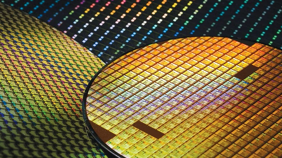
Siemens and TSMC are working on next-generation process nodes, including 3nm, 2nm, A16, and A14 technologies. Siemens’ Calibre nmPlatform is certified for these nodes, while the Solido Simulation Suite is certified for SPICE accuracy on N3A, N2P, A16, and A14 process technologies. These tools support design and verification of analog, mixed-signal, RF, standard cell, and memory circuits on TSMC process nodes.
The collaboration includes TSMC’s A14 custom design reference flow (CDRF), where the Solido Simulation Suite performs reliability-related simulations, including IC aging, self-heating, and safe operating area (SOA) checks. The A14 flow also incorporates the Solido Design Environment for variation-aware verification, sensitivity analysis, and automated cell optimization.
Siemens’ mPower Analog is certified for transistor-level EM/IR sign-off on TSMC’s N2P process. Siemens’ Aprisa software has achieved TSMC N2P Integrated Tool Certification for digital implementation flows, confirming support for design implementation at the N2P node.
Siemens tools support design, implementation, and verification of TSMC Compact Universal Photonic Engine (COUPE) technology. Joint silicon photonics work includes flow development using Innovator3D IC, Calibre 3DStack, L-Edit, Solido Simulation Suite, and Calibre Interactive software.
Source: Siemens
About Siemens Digital Industries Software
![]()
Siemens Digital Industries Software, a business unit of Siemens AG, provides industrial software, hardware and related services through the Siemens Xcelerator platform. The company’s portfolio includes product lifecycle management, electronic design automation, simulation and digital twin tools, manufacturing operations management and low-code application development. These products support design, engineering and production workflows across sectors such as aerospace and defense, automotive, electronics and semiconductors, machinery, medical devices and process manufacturing. Siemens Digital Industries Software traces its origins to 1963 as United Computing, later becoming Siemens PLM Software in 2007 before adopting its current name. It supplies technologies that help organizations manage product, process data, and improve development and manufacturing efficiency across a range of industrial applications.
About TSMC

Taiwan Semiconductor Manufacturing Company (TSMC) is the world’s largest dedicated semiconductor foundry, based in Hsinchu, Taiwan. Founded in 1987, TSMC developed the pure-play foundry business model and has become a key player in the global chip supply chain. The company manufactures advanced semiconductor components using process technologies like 5nm and 3nm nodes, with plans to move to 2nm and smaller. TSMC serves customers across industries like consumer electronics, computing, automotive, networking, and industrial applications. Major technology firms rely on TSMC to produce chips for smartphones, data centers, AI systems, and autonomous vehicles. By the end of 2024, TSMC employed about 84,000 people worldwide. The company served 530 customers and approx.. 12,000 products for various applications.