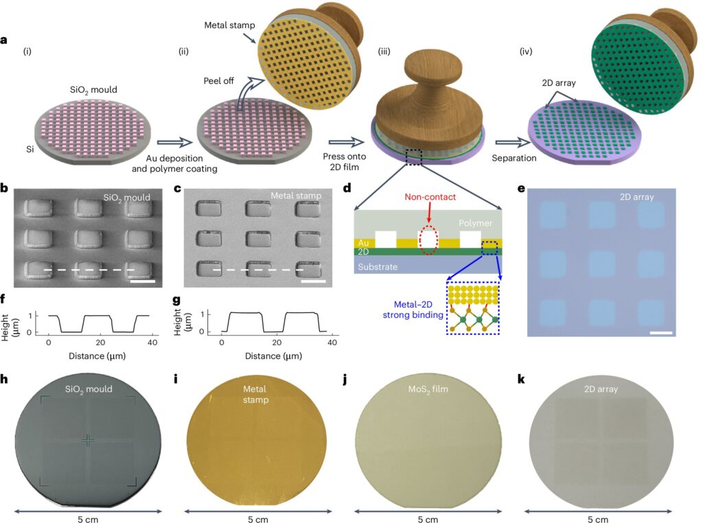
Researchers at Nanyang Technological University (NTU) have developed a residue-free metal-stamp imprinting method that can directly pattern 2D semiconductor films into wafer-scale arrays, minimizing damage and contamination, key challenges in current processes, tells this article on Tech Xplore.
Rather than relying on chemical etching or polymer masking, the team uses a 3D-morphology metal stamp pressed onto a grown 2D film (e.g., MoS₂). Parts of the film in contact with the stamp are selectively exfoliated, leaving behind a clean, patterned array on the substrate. Detailed spectroscopy and microscopy verify that there is no damage to the crystal or residue.
To validate performance, NTU produced MoS₂ transistors and logic circuits on 2-inch wafers, achieving 97.6% device yield and 20× lower threshold-voltage variation compared with reactive-ion-etching patterned devices.
Why This Is Important to Engineers and Fabrication Experts:
- Integrating with semiconductor fab lines is made possible by clean, scalable patterning that stays away from chemicals and polymers.
- High yield and uniformity: Reliability in manufacturing is enhanced by consistent device performance across wafers.
- Superior electrical properties: Logic and sensor circuits constructed using 2D semiconductors require predictable, robust device behavior, which is made possible by reduced variability.
This breakthrough offers a scalable alternative to conventional patterning tools, accelerating the path toward industrial-scale integration of 2D materials. The method holds promise for building next-gen electronics—from flexible transistors to optoelectronic chips—that leverage the unique properties of atomically thin semiconductors without compromising quality or yield.