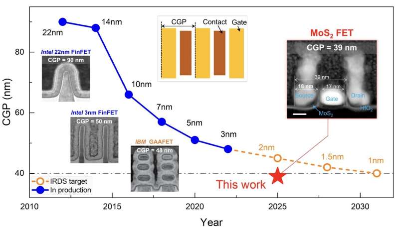
Researchers led by Nanjing University have developed a technique that directly grows ultra-small, high-performance electronic components on two-dimensional semiconductor materials, an advance that could push device miniaturization deeper and improve performance at nanoscales, tells Tech Xplore. This work centers on attaching electrical contacts at extremely small dimensions to 2D semiconductors such as molybdenum disulfide (MoS₂), a material of interest because of its potential to replace or supplement silicon in future electronics.
As electronic devices shrink to the 1-nanometer node and beyond, forming reliable ohmic contacts, connections that allow current to flow freely, becomes increasingly difficult. Traditional approaches struggle with rising contact resistance as dimensions fall, limiting performance. The research team addressed this by using molecular beam epitaxy (MBE) to grow crystalline semimetallic antimony directly on a monolayer of MoS₂. This bottom-up growth method yields ultra-short, low-resistance contacts that remain well-attached to the 2D material even at scales relevant for next-generation transistors.
The ability to integrate contacts at such small scales matters because contact resistance and device size are major constraints on performance as devices shrink. Contacts grown directly on the semiconductor maintain intimate atomic contact and provide a pathway for current with minimized resistance. That, in turn, supports the creation of transistors and other components that operate efficiently at nanoscale dimensions.
MoS₂ and other 2D semiconductors have layered structures only a few atoms thick, offering benefits such as potentially high switching speeds and low power consumption compared with bulk materials. But practical circuits require not just an active channel but also dependable ways to inject and extract charge. By combining 2D channels with grown contacts, the researchers point to a route for building components that could meet the performance and size demands of future electronics.
This advance is an important step toward integrating 2D materials into mainstream semiconductor technology, though further work will be needed to scale manufacturing and fully assess performance in complex circuits.