University of Wisconsin–Madison engineers have designed a semiconductor imaging system that converts near-infrared light into visible wavelengths without needing a power source, a breakthrough for sensing and imaging technologies. Near-infrared spans roughly 750–1,400 nanometers and carries information that visible light cannot. It’s important in applications such as food inspection, pharmaceuticals, machine vision, agriculture, night vision, and more, but typical systems that detect this band rely on powered electronics or intensive illumination to function. The new system overcomes these limitations by enhancing a passive up-conversion method that turns low-energy near-infrared photons into higher-energy visible photons through internal quantum processes.
The research team, led by PhD student Rabeeya Hamid with faculty support from Professor Mikhail Kats and collaborators at Stanford University and Argonne National Laboratory, focused on strengthening the efficiency of the triplet-triplet annihilation process in organic semiconductors. In this process, near-infrared photons excite electrons to a low-energy state; two such excitations then combine to produce a single higher-energy photon in the visible spectrum. Passive conversion has been studied for years, but it has historically struggled with weak output at useful imaging intensities. The team’s approach used nanoscale engineering to boost both absorption and emission in thin films of organic semiconductor materials.
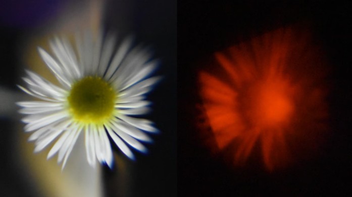
Two key enhancements drove the performance gains. A back-reflective dielectric coating increased emitted light by about 2.5 times, while a layer of gold nanopillars doubled the capture of incoming near-infrared light through plasmon resonance effects. Combined, these structures quadrupled the visible image intensity compared with earlier passive systems, rivaling some powered commercial detectors at selected infrared wavelengths. The result is a clear, power-free imaging signal at intensities far lower than other passive technologies can handle.
The researchers report their results in Advanced Functional Materials and see more work ahead to broaden sensitivity across the full near-infrared range and move toward practical devices.