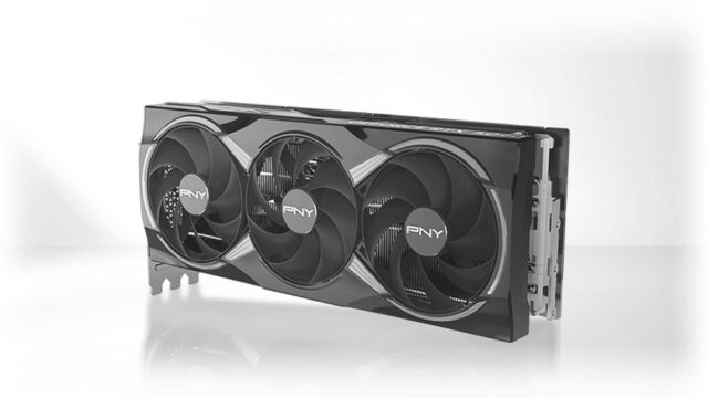
AUSTIN, TX, Jan 24, 2025 – BOXX Technologies has announced that, as a supplier of NVIDIA-Certified Systems, select BOXX products will support the new NVIDIA GeForce RTX 50 Series GPUs available as of date. The new NVIDIA Blackwell architecture GPUs combine the latest-generation RT Cores and Tensor Cores with GDDR7 memory, increased clock speed, and VRAM, to deliver improved AI, graphics, rendering, and ray-tracing performance.
“Our support for the latest NVIDIA GeForce RTX 50 Series technology is essential because these GPUs accelerate application performance and creative workflows,” said BOXX CEO Kirk Schell. “Now video editors, VFX artists, animators, architects, and other content creators can take advantage of all AI has to offer and design, render, collaborate, and meet project deadlines faster than ever before.”
The NVIDIA GeForce RTX 50 Series GPU supported by BOXX systems features the latest Blackwell technology for accelerated AI and ray tracing, as well as up to1.8TB/s of GDDR7 memory bandwidth to power:
Faster content creation
Multi-application workflows
Improved AI and machine learning support
The new GPU series also offers 33% more VRAM than the previous generation, enabling users of Adobe Creative Cloud, DaVinci Resolve, Cinema 4D, Revit, Rhino, and other applications supported by NVIDIA Studio Drivers, to optimize creative tasks like:
Next-gen raytracing & AI-powered graphics
AI-assisted video editing and rendering
Real-time 8K video editing
To accelerate V-Ray, Autodesk Arnold, Lumion, and other 3D renderers supported by NVIDIA Studio Drivers, the new NVIDIA GeForce RTX 50 Series GPUs inside BOXX systems feature DLSS 4 with Multi Frame Generation which also delivers superior image quality by multiplying frame rates by up to eight times over traditional rendering.
“Demanding graphics and workflows require powerful, purpose-built solutions,” added Schell, “and NVIDIA GeForce RTX 50 Series GPUs supported by innovative BOXX solutions give creators the performance they need to run the latest 3D and AI-accelerated applications.”
About BOXX
Founded in 1996 and headquartered in Austin, Texas, BOXX Technologies specializes in high-performance computer workstations tailored for professionals in architecture, engineering, product design, visual effects, animation, and data science. Their product lineup includes deskside and rack-mounted workstations, rendering systems, and servers, all designed to accelerate workflows in industries such as media and entertainment, manufacturing, and government. BOXX’s APEXX series, for instance, offers performance-tuned, liquid-cooled systems featuring the latest Intel Core Ultra and AMD Ryzen processors, delivering unparalleled speed and reliability. The company maintains its design, manufacturing, and support operations at its Austin headquarters, ensuring quality control and customer service excellence. With a global presence through 40 international resellers, BOXX provides purpose-built solutions that enhance productivity and meet the demanding requirements of creative professionals worldwide. As of 2024, BOXX Technologies employs approximately 67 individuals and has an estimated annual revenue of $24.1 million.
LONDON, UK, Jan 24, 2025 – Stelia has announced the appointment of David Hughes as VP of engineering. David brings experience in developing and scaling high-traffic, low-latency and big-data platforms and software engineering with a focus on network and storage appliances.
David will lead Stelia’s platform strategy, guide the creation of AI-driven networking technologies, and scale the engineering team up to meet the company’s goals. His experience includes building large-scale networks, reliable platforms, and robust infrastructure. He will help Stelia improve data movement, connect diverse AI resources, and simplify distributed AI operations.
This leadership appointment comes at a crucial time, as AI infrastructure faces significant challenges. With NVIDIA’s flagship H100 chip priced at $25,000 each and 8 chips per server chassis, efficient utilization is critical.
AI systems rely on large amounts of data, with global data center storage expected to increase from 10.1 zettabytes in 2023 to 21 zettabytes by 2027. Experts estimate that by 2025, AI will account for most network application traffic, with about 75% of all network traffic involving AI by 2030. Managing these changes requires engineering leaders who understand the growing demands of AI technology.
“We are thrilled to welcome David to the team,” said Tobias Hooton, CEO, Stelia. “His expertise as a technologist spanning multiple domains, coupled with a deep involvement and commitment to open source technology and communities, will be invaluable as we continue to push the boundaries of AI innovation and empower enterprises to drive transformative change.”
Prior to joining Stelia, David served as CTO at Genesis Cloud, where he led engineering and technology, product development and infrastructure operations. More importantly, David managed the transition from being a consumer/enthusiast-centric GPU cloud service provider to an accelerated compute platform for enterprise. He also brings experience in cloud computing, big data, HPC, web hosting and lots more across a range of markets. Recently, David was part of the unicorn startup Adjust GmbH.
“I’m excited to join Stelia at such a pivotal time,” said Hughes. “The opportunity to expand and lead a world-class engineering team and drive AI acceleration aligns perfectly with my passion for being at the coalface of the industry and solving problems that unlock massive opportunity for the wider industry. More importantly the opportunity to leave a lasting mark on computing, similar to Scott McNealy’s “change computing forever” mentality. I look forward to working with the talented team at Stelia to build and scale AI solutions that make a lasting impact.”
About Stelia
Stelia.io, founded in 2021 and headquartered in London, UK, is a global connectivity company that supports emerging technology businesses and enables innovation. The company specializes in developing ultra-fast, flexible, and scalable data mobility platforms tailored for AI applications. Stelia’s mission is to empower AI builders with the infrastructure and connections essential for widespread AI adoption. Their platform offers ultra-low latency of less than 1 millisecond and terabit-scale bandwidth, ensuring seamless access to cutting-edge AI and machine learning resources, including AI storage platforms, GPU clouds, and public clouds. This enables businesses to accelerate AI innovation, enhance infrastructure, and connect distributed systems across various industries. The company is funded by venture capital, securing seed funding in 2024.
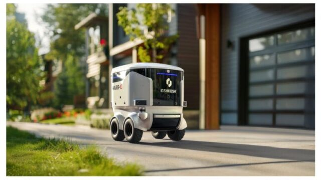
LAS VEGAS, NV, Jan 24, 2025 – Oshkosh Corp. announced that it was selected as a winner in this year’s CES Picks Awards. Oshkosh was recognized for its Hail-able Autonomous Refuse Robot – Electric or HARR-E.
With HARR-E, Oshkosh is pioneering a new way to tackle a weekly chore — taking out the trash. HARR-E is an autonomous, electric refuse collection robot that offers on-demand refuse and recycling pickup via a smartphone app or virtual at-home assistant. Using AI-enabled navigation and advanced sensors, HARR-E autonomously collects trash and then returns to a central collection area.
Using advanced AI and robotics, Oshkosh’s Pratt Miller unit created a prototype system to improve efficiency and streamline logistics. The system enhances traditional refuse collection services, offering modern solutions for planned communities and businesses.
“Self-driving technology will play an increasing role in our daily lives. HARR-E is a great example of how autonomous technology can make chores like taking out the trash a thing of the past,” said Jay Iyengar, executive vice president, chief technology and strategic sourcing officer, Oshkosh Corp. “The Oshkosh team is proud to be recognized with this prestigious honor, as we continue to develop innovative solutions in electrification, AI, autonomy and connectivity to help keep communities clean and support a sustainable future.”
The awards’ editorial team shared, “The Picks Awards recognize outstanding products across consumer technology, the custom installation industry and innovative new technology that can truly help businesses of all sizes across various industries. Our team was highly impressed by the excellence and scope of this year’s entrants. All the winners should be proud of their achievements – a well-deserved congratulations from the entire awards team.”
Making its debut at CES 2025, Oshkosh announced electrification, AI, autonomy and connectivity solutions to help everyday heroes — such as firefighters, soldiers, postal carriers, construction workers and people doing tough work on the tarmac of an airport — and the communities they serve. These solutions include:
A first-of-its-kind, purpose-built, all-electric refuse and recycling front-loader vehicle along with AI and electrified technologies that improve refuse and recycling collection in neighborhoods.
Autonomous robot designed for on-demand refuse collection to help manage weekly chores.
AI-enabled Collison Avoidance Mitigation System (CAMS) for fire and emergency vehicles to provide critical advance notice of an impending collision to first responders.
Self-driving vehicles and connected solutions like iOPS and ClearSky Smart Fleet technologies to improve operations at airports and on job sites.
About Oshkosh
Founded in 1917 and headquartered in Oshkosh, Wisconsin, Oshkosh Corporation is a global industrial technology company specializing in the design and manufacture of purpose-built vehicles and equipment. The company operates through four primary business segments: Access Equipment, Defense, Fire & Emergency, and Commercial. Its diverse product portfolio includes aerial work platforms, tactical military vehicles, firefighting apparatus, and refuse collection trucks. Serving industries such as construction, defense, emergency services, and waste management, Oshkosh Corporation employs approximately 17,300 people worldwide. In 2023, the company reported revenues of $9.7 billion, a 17% increase from the previous year. Recent innovations include the development of electric vehicles and AI-powered systems, such as plug-in fire engines and autonomous garbage collection robots, underscoring the company’s commitment to advancing technology in specialty vehicles.
The hardware that makes AI possible is hidden away in data centers, huge non-descript buildings that, because of security concerns, may not reveal their purpose. But their thermal signature is a dead giveaway. So much energy is needed to cool down the servers inside that future mega-sized data centers must be big energy production facilities, such as hydroelectric dams. That may not be enough. They are on the verge of bringing back nuclear reactors.
To counter the surge required by present and future data centers is a small but growing movement to reduce the need for computing done by data centers. By doing the computing on the edge, rather than in the (data) center, could we not stop the madness of building ever bigger data centers? OpenAI, the company that created ChatGPT, has plans to build several 5 GW data centers, 30 times the size of the biggest data centers currently in existence. 5 GW is roughly the amount of energy all of Iceland consumes in a year!
The argument for more edge processing is sound. Sensors, such as those in consumer devices and industrial equipment, emit a steady stream of data that is currently processed by hordes of GPUs on neural network chips in data center servers. These servers are always on, always demanding energy and generating heat. Yet, most of the data they are processing is just noise.
Filtering out the noise at the edge makes sense. And if the useful signal remaining could be processed on the edge, we could actually downsize our need for data centers.
That’s the theory behind a new crop of small spiking neural processors (SNPs) in a nutshell – literally. A nutshell could actually hold several SNPs.
Hey, Buddy. Want to Buy a SNP?
I was shown my first SNP in a hotel room.
I meet Innatera’s chief commercial officer, Shreyas Derashri and CEO, Sumeet Kumar, in a suite at the Venetian Hotel in Las Vegas. As companies sometimes do, Innatera has booked a room instead of a booth on the show floor. Smart. They have my undivided attention. The show floors are a circus. A suite lets the company set up rooms for different applications of their chip.
A paperweight to thank me for visiting? Look closely. What appears to be a gold flake is the smallest of SOCs (systems on a chip), measuring just 6 X 6 mm.
The Innatera team has traveled to Las Vegas from HQ in Delft, Netherlands, to show off the first-ever always-on spiking neural processor, the T1. Tiny beyond belief, just 6mm square, the T1 is indeed a marvel of miniaturization. Its diminutive size gives it a big advantage over NVIDIA’s processors on the big stage at CES. Yet, this little chip can do quite a bit of what its more famous counterpart can do with just 1/500 the power.
What Can It Do?
The T1’s lower-than-low power consumption opens up a flood of new product improvements. Think of portable devices, such as smartphones, wearables (like Fitbit and smartwatches), smart speakers, and smart appliances, hundreds of which are on display a few floors below, all able to last for weeks or months without being recharged or having to replace their batteries. Think also of commercial buildings and smart homes loaded with battery-operated smart and connected devices, such as doorbell cams, smoke alarms, thermostats, people counters, security systems, etc., that don’t have to be wired or have their batteries changed from the top of tall ladders.
In all these smart devices, sensors abound. A home smart speaker may have two sensors, a commercial building, hundreds. Innatera estimates that four billion smart devices will be added each year.
I am reminded of my smart doorbell, which seems to run low on charge at the most inopportune times, such as during my vacation, and uses its precious battery to inform me of stray cats, blowing leaves, passing cars, and other things I care little about. Could it just let me know of package delivery or who is ringing the bell?
How SNPs Work
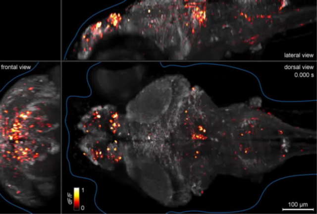
Neurons firing in a fish brain is an example of a biological spiking neural network.
A spiking neural processor, such as the one developed by Innatera, is inspired by the functioning of biological neurons in the brain. Instead of continuously processing information like traditional neural processors, SNPs become active only when they encounter discrete, event-driven signals called “spikes,” e.g., a change in input signal or sensor data. This mimics how biological neurons fire in response to stimuli. The spikes, which carry information, are recorded temporally (via timing and sequence) rather than in continuous values. SNPs ignore the ever-present noise altogether, much as your brain ignores the sensations of the shirt on your back.
SNPs excel at real-time processing of sensory data, such as audio, visual, or tactile inputs, with minimal latency. We see an example of a song being recognized by its audio signature at the sensor. This makes SNPs suited for the recognition of complex data patterns more effectively, particularly in environments where data is sparse and episodic.
Living on the Edge
Innatera’s SNP’s are fundamentally different and more efficient for specific tasks compared to the GPU-based architectures used for large language models (LLMs) that, by comparison, consume unnecessary energy since they are always on and always processing.
Innatera’s chips are designed to work on the edge, in remote areas where power is scarce and what little power is needed can be supplied by batteries.
Edge processing not only saves the energy typically required to transmit data from the field to the data center, but it also eliminates latency, delivering output for AI systems without pause. Neural processors, because of their energy requirements, require them to be plugged in and, therefore, can be far from sensors. This causes latency problems.
The Innatera T1 SNP SoC requires less than 10 mW of power. Being such a little drain on a battery lets a remote sensor operate for months.
The TI SNP is able to filter the waving leaves of a houseplant from a room cam.
Innatera showed applications of the use. There was a people counter by which an FIR (far infrared sensor) backed by an SNP was able to process the thermal shapes of people in the room. In another room, a radar system was able to filter out the leaves of a houseplant being blown around by a fan. Both applications ensure privacy and minimize power use as they process entirely on the device, and images are of low resolution, unlike vision-based systems.
Innatera vs NVIDIA and Unfair Comparison
NVIDIA neural processors differ significantly from Innatera spiking neural processors. Nvidia’s A100 and H100, for example, are general-purpose AI processors optimized for matrix computations. NVIDIA has explored neuromorphic computing but focuses on simulating SNPs on GPUs rather than building dedicated neuromorphic chips. Compared to Innatera chips, NVIDIA GPUs are larger and consume much more power (100–700 W) than Innatera SNPs.
And then there is the cost. NVIDIA’s H100 costs roughly $25,000 each. (Innatera has not yet released pricing for the T1 SNP).
The Competition
NVIDIA offers low-power chips meant for edge use, such as their Nano and Xavier. Still, with power consumption of 10W and 30W, respectively, there is no comparison to the Innatera’s sub-milliwatt chip.
Innatera is not alone in making spiking neural network chips for edge devices, but a quick survey of the competition showed Innatera to be among the smallest and most energy efficient.
Intel has the Loihi, which operates at relatively low power for its capabilities (~50 mW per chip under typical workloads. IBM’s TrueNorth, with its simulation of a million neurons, a large form factor, and 70 mW power consumption, is better deployed in a data center or research applications than on the edge.
GrAI Matter Labs GrAI One chips are larger than Innatera’s chips as they prioritize computational capabilities for edge-cloud hybrid systems and are more power-hungry, requiring a slightly higher power level (10–50 mW)
SynSense chips are compact and tailored for real-time sensory processing, making them similar in size to Innatera’s chips. Their Dynap-SE consumes around one mW for sensory processing tasks, comparable to Innatera’s chips. SynSense emphasizes vision-based tasks, while Innatera is versatile across sensory modalities like sound, motion, and biological signals.
BrainChip’s Akida AKD100 “reference chip,” which uses Akida’s “neuron fabric” may be Innatera’s closest competition.
About Innatera Nanosystems
Sumeet Kumar, CEO of Innatera, at CES 2025.
I wrap up the meeting with a brief chat with Dr Sumeet Kumar. Dr Kumar earned both his master’s and PhD in microelectronics from Delft University of Technology in the Netherlands. He went on to manage research programs at Delft aimed at developing next-generation compute hardware for highly automated vehicles. Dr Kumar worked at Intel, focusing on developing domain-specific tools for complex media processor architectures. He founded Innatera in 2018.
Dr Kumar is a gentleman, pleasant, well dressed and exudes an air of quiet confidence. We expect someone who thinks on the scale of microns but Dr Kumar thinks of the whole world. He explains how SNPs like Innatera’s, small as they are, could affect climate change. By simply ignoring the torrent of noise from sensors and processing only spikes at the edge, current data centers would be relieved and produce less heat. Data centers working at less than full capacity would obviate the need for more data centers.
The Dutch-based Innatera Nanosystems was spun out of Delft University of Technology in 2018 to develop ultra-low power neuromorphic processors that mimic the brain’s mechanisms for processing sensory data. The company is headquartered in Rijswijk, Netherlands and maintains a design center in Bangalore, India.
Innatera has over 80 employees. It is a private company and, as such, is not required to disclose revenue.
Innatera raised a total of €25 million in funding over two rounds. In November 2020, the company secured €5 million in seed funding. This round was led by Munich-based deep-tech investors MIG Verwaltungs AG and the Industrial Technologies Fund of btov.
In 2024, Innatera raised an additional €20 million in an oversubscribed Series A funding round, including investments from Invest-NL Deep Tech Fund, the EIC Fund, MIG Capital, and Matterwave Ventures.
SUNNYVALE, CA, Jan 23, 2025 – Numem is present at the Chiplet Summit to showcase its high-performance solutions in chiplet architectures. By accelerating data delivery via new memory subsystem designs, Numem solutions are re-architecting the hierarchy of AI memory tiers to eliminate the bottlenecks that negatively impact power and performance.
The increasing demand for AI workloads and processors, including GPUs, is exacerbating the memory bottleneck. This issue arises because SRAM and DRAM are improving at a slower pace in terms of performance and scalability, limiting system performance. To address this, memory solutions with higher bandwidth and power efficiency are required, along with a reevaluation of traditional memory designs.
Numem is transforming traditional memory paradigms with its advanced SoC Compute-in-Memory solutions. Built on its patented NuRAM (MRAM-based) and SmartMem technologies, the innovations tackle critical memory challenges head-on. The result is a groundbreaking approach to scalable memory performance, built to meet HPC and AI application needs.
“Numem is fundamentally transforming memory technology for the AI era by delivering unparalleled performance, ultra-low power, and non-volatility,” said Max Simmons, CEO of Numem. “Our solutions make MRAM highly deployable and help address the memory bottleneck at a fraction of the power of SRAM and DRAM. Our approach facilitates and accelerates the deployment of AI from the data center to the edge, opening up new possibilities without displacing other memory architectures.”
MRAM-Based Chiplet Solution
At the Summit, Numem is showcasing innovative chiplets – nonvolatile, high-speed, ultra-low power solutions that leverage MRAM to overcome memory challenges in chiplet architectures. Sampling is expected to begin in late Q4’25.
Key features and benefits include:
Unparalleled Bandwidth: Delivers up to 4TB/sper 8-die memory stack, exceeding existing AI memoryHBM solutions.
High Capacity: Supports 4GB per stack package, enabling scalability for demanding AI workloads.
Nonvolatile with SRAM-Like Performance: Combines ultra-low read/write latency with persistent data retention, offering reliability and efficiency. Provides the scalability and power needed to address the demands of future AI and data-centric workloads.
Power Smart: Game-changing power efficiency and AI Edge and Data Center based solutions with the ability to implement multi-state flex power functions (active/standby/deep sleep).
Broad Application Compatibility: Optimized for AI applications across OEMs, hyperscalers, and AI accelerator developers to drive the adoption of chiplet-based designs in high-growth markets. Designed with standard industry interfaces such as UCIe to facilitate ecosystem compatibility.
Advanced Integration: Complement other chiplet components (e.g., CPUs, GPUs, and accelerators).
In-Compute Intelligence: Improves memory performance by handling data flow, optimizing read/write speeds, adjusting power settings, and enabling self-testing features.
Proven Technology: Advanced memory subsystem IP based on proven foundry MRAM process. Offers radiation performance that mitigates exposure to soft errors.
Numem is also demonstrating its patented NuRAM/SmartMem technology, that achieves significantly faster speeds, lower latency and dynamic power consumption compared to other MRAM solutions. It reduces standby power by up to 100x compared to SRAM, with similar bandwidth, and delivers up to 4x faster performance than HBM while operating at ultra-low power.
Demonstrations will be given in Numem’s booth #322 on the show floor of the Santa Clara Convention Center from Jan 21-23, 2025.
MICKINNEY, TX, Jan 23, 2025 – Sigmetrix has announced their latest release of CETOL 6σ tolerance analysis software, version 12.0, available for immediate download. Tolerance analysis offers several advantages for businesses. It supports higher profits by balancing product quality with production costs. Companies can speed up product launches by reducing the need for additional design or prototype stages. It also allows teams to make informed product and process decisions before making costly investments.
CETOL 6σ enables product development teams to understand the often-complex impact of dimensional and assembly variation easily and fully on their designs. This knowledge enables them to make the proper adjustments before problems appear in manufacturing or, even worse, in their customers’ hands. Users of all expertise levels will appreciate the multiple levels of assistance available within the software. This new release of CETOL 6σ builds upon the features already in place and adds improvements, including:
A New Version of the Software Directly Integrated with Siemens NX– CETOL 6σ users will have the option of using CETOL 6σ as an add-in application within the NX environment, supporting the additional capabilities of saving the CETOL 6σ data embedded within the NX files as well as automatically pushing changes to linked tolerance values back to the PMI in NX. The standalone version of CETOL 6σ for NX is available as well to facilitate migration to the new solution, as data from the standalone version may be opened in the new, integrated version.
Select Auxiliary Features for Other Conditions – Auxiliary Features, functionality first added in 3, may now be referenced to modify the location of measurement endpoints, to modify the location of a joint, or to modify the location of a feature origin.
Reset Joint DOFs – CETOL 6σ has applied an algorithm to automatically set degree-of-freedom controls for joints being imported or manually added based on the order in which they are added. Adjusting the setting when the order wasn’t correct, though, is now much faster with this new context menu option.
Add Geometric Tolerance Context Menu Option—This feature allows the user to add a geometric tolerance directly from the context menu for the feature in addition to the standard tool in the ribbon.
Upload to VariSight – Uploading data to VariSight, a new, enterprise-level product for managing CETOL 6σ data files schedule to be released later this year, is supported directly within the application.
As with prior releases, CETOL 6σ v12.0 is available in English, Japanese, and Simplified Chinese.
Sigmetrix director of customer success and product strategy, Stephen Werst, commented, “CETOL 6σ v12. is a significant step forward for Sigmetrix as we strive to achieve feature parity across all supported CAD platforms, continue to make the software easier to use, and prepare for the upcoming release of our newest product, Varisight. This release, along with improvements in our entire product portfolio, continues our unrelenting efforts to help companies build better products through mechanical variation management via a robust combination of software, training, and consulting services.”
PARIS, France, Jan 23, 2025—Bluebeam, part of the Nemetschek Group, announces its plan to invest in and accelerate its expansion into France in 2025.
“France’s overall economic strength and stability make it one of the top economies in the world,” said Amit Sangal, chief growth officer of Bluebeam and the Nemetschek Group Build & Construct Division. “Construction and design professionals face challenges such as labor shortages, regulatory complexities, and barriers to technology adoption. Bluebeam, with its focus on improving collaboration, streamlining workflows, and digitizing processes, is well-positioned to help address these challenges and drive efficiency in France and beyond.”
Charles Parissier Source: LinkedIn
As part of this expansion strategy, Bluebeam announces the appointment of Charles Parissier to lead operations in France as Bluebeam country manager. With over 15 years of industry experience, including at ALLPLAN France, Charles Parissier will oversee sales and business development to drive growth and deliver value to customers. Bluebeam also plans to expand its headcount to support and enhance the quality of service offered to users in the region.
“We’re thrilled to introduce Bluebeam’s innovative solutions to construction professionals in France, a market full of growth potential,” said Charles Parissier, Bluebeam country manager for France. “The strength of Bluebeam’s digital productivity and collaboration capabilities combined with the support of the Nemetschek Group, uniquely positions us to drive adoption and foster innovation that will help transform the French architecture, engineering and construction industries.”
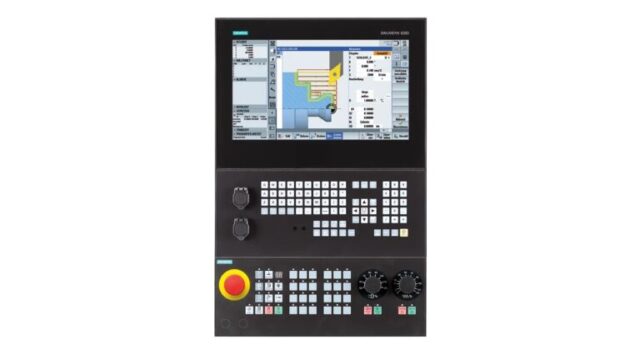
BENGALURU, India, Jan 23, 2025 – Siemens announced the launch of MACHINUM at IMTEX 2025. MACHINUM has the potential to reduce machine tool setup time up to 20% and cycle times and energy consumption up to 18%.
Image Source: Siemens
Investment in India’s high-end manufacturing for local and export markets is driving changes in the machine tool market. Advanced technologies are being adopted to support this growth. The demand for modern machine tools is growing due to the need for precision, customization, and technology integration in manufacturing processes.
Achim Peltz, CEO of Siemens Motion Control, digital industries, Siemens AG, “As one of the technology players with integrated solutions across the entire value chain, one of our prime focus areas is to support the accelerated adoption of digitalization and help the industry move up the value chain through co-creation. With the launch of the MACHINUM portfolio, we are shaping the sustainable, digital, and future-proof transformation of the machine tool manufacturing ecosystem in India.”
MACHINUM is an integral part of Siemens Xcelerator, the open digital business platform that includes a portfolio of software and IoT-enabled hardware, an ecosystem of partners, and a marketplace. MACHINUM helps machine tool companies and scale digital transformation in both manufacturing and design processes.
Siemens will also showcase the upgraded 5th generation SINUMERIK 828D, paving the way for SINUMERIK Run MyVirtual Machine. This innovative feature allows NC programs to be created, validated, and optimized using a digital twin of the machine without interrupting production, reducing setup time on the real machine by up to 20% and minimizing production risks. With features like digital twin readiness, effortless HMI customization, and 40% faster program buffering, it simplifies operations and improves efficiency. The high-resolution display ensures clear operator visibility, while robust cybersecurity, including IEC 62443 compliance, safeguards systems from threats.
Vijay Pratap Singh, Head of Motion Control, digital industries, Siemens Limited, said, “Our energy-efficient hardware, operational technology, and digitalization are key to boosting sustainability in machine tool manufacturing. At IMTEX 2025, we will not only showcase our components with high energy efficiency and lower carbon footprint but also applications to compensate, recover, and limit the energy consumed. Such a seamless portfolio helps machine tool manufacturers and users save costs while being more productive with fewer resources.”
KURIM, Czech Republic and LINARES, Spain, Jan 23, 2025 – MCAE Systems and Meltio has announced that MCAE Systems will play a key role as an official sales partner in the distribution and support of Meltio metal 3D printing solutions in the Czech and Slovak markets. The main goal will be to boost growth in the Czech and Slovak metal additive manufacturing markets.
Meltio provides a metal 3D printing solution designed for industrial use. It uses welding wire, the most cost-effective metal feedstock available.
MCAE Systems will focus on building a supportive ecosystem for Meltio’s technology in the Czech and Slovak territories. It will partner with and drive business opportunities alongside technology centers, tooling machine companies, robotic integrators, academia, and industry.
“In nearly 30 years of working with 3D technologies, we have built a strong position in the market and a deep understanding of our customers’ needs. The partnership with Meltio will allow us to combine many years of experience in both 3D printing and CAD/CAM and production on CNC machines and robots. Laser metal welding technology perfectly complements our wide portfolio of professional manufacturing technologies and we are convinced that it will open up new application possibilities in the field of metal 3D printing for our customers,” says Miloslav Drápela, CEO of MCAE Systems.
Francisco González, Head of EMEA at Meltio highlights the significance of this partnership, stating, “We are thrilled to be working with and this collaboration between MCAE Systems us serves as a great indicator of how Meltio’s partner ecosystem and our unique wire-laser metal 3D printing technology for industries is evolving in Czech Republic and Slovak markets booth our metal AM solutions in the east of Europe.” And he added: “Together, we will be able to cater to the ever-growing interest in Meltio’s technology and its applications for different industries and reliable metal applications.”
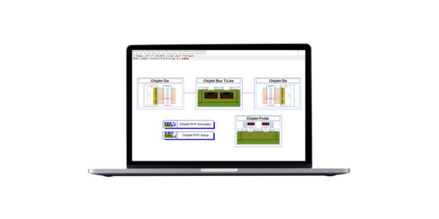
SANTA ROSA, CA, Jan 23, 2025 – Keysight Technologies has announced the launch of Chiplet PHY Designer 2025, its latest solution for high-speed digital chiplet design tailored to AI and data center applications. The enhanced software introduces simulation capabilities for the Universal Chiplet Interconnect Express (UCIe) 2.0 standard and adds support for the Open Computer Project Bunch of Wires (BoW) standard. As an advanced, system-level chiplet design and die-to-die (D2D) design solution, Chiplet PHY Designer enables pre-silicon level validation, streamlining the path to tapeout.
As AI and data center chips grow more complex, ensuring reliable communication between chiplets becomes crucial for performance. The industry is addressing this challenge through open, emerging standards like UCIe and BoW that define the interconnects between chiplets within an advanced 2.5D/3D package. When designers use these standards and ensure chiplets meet compliance, they help expand chiplet interoperability while lowering development costs and risks in semiconductor development.
Key Benefits of the Chiplet PHY Designer 2025:
Ensures Interoperability: Verifies designs meet UCIe 2.0 and BoW standards, enabling seamless integration across advanced packaging ecosystems.
Accelerates Time-to-Market: Automates simulation and compliance testing setup, such as Voltage Transfer Function (VTF), simplifying chiplet design workflows.
Improves Design Accuracy: Provides insight into signal integrity, bit error rate (BER), and crosstalk analysis, reducing risks of costly silicon re-spins.
Optimizes Clocking Designs: Supports advanced clocking scheme analysis, such as quarter-rate data rate (QDR), for precise synchronization in high-speed interconnects.
Hee-Soo Lee, high-speed digital segment lead, Keysight EDA, said: “Keysight EDA launched Chiplet PHY Designer one year ago as the industry’s first pre-silicon validation tool to provide in-depth modeling and simulation capabilities; this enabled chiplet designers to rapidly and accurately verify that their designs meet specifications before tapeout. The latest release keeps pace with evolving standards like UCIe 2.0 and BoW while delivering new features, such as the QDR clocking scheme and systematic crosstalk analysis for single-ended buses. Engineers using Chiplet PHY Designer save time and avoid costly rework, ensuring their designs meet performance requirements before manufacturing. Early adopters, like Alphawave Semi, attest that Chiplet PHY Designer ensures seamless operation and interoperability for 2.5D/3D solutions available to their chiplet customers.”